At its core, a CVD furnace functions like a highly specialized oven that uses chemical reactions to deposit a solid, ultra-thin film onto a surface. It works by introducing specific precursor gases into a heated chamber containing the object, or substrate, to be coated. The high temperature causes these gases to react or decompose, and the resulting solid material "grows" onto the substrate's surface, creating a new layer with precisely controlled properties.
Chemical Vapor Deposition (CVD) is not just about coating a surface; it's a process of atomic-scale construction. Its success hinges on a single principle: absolute control over the reaction environment—temperature, pressure, and gas chemistry—to build a perfect, uniform solid film from a gaseous state.
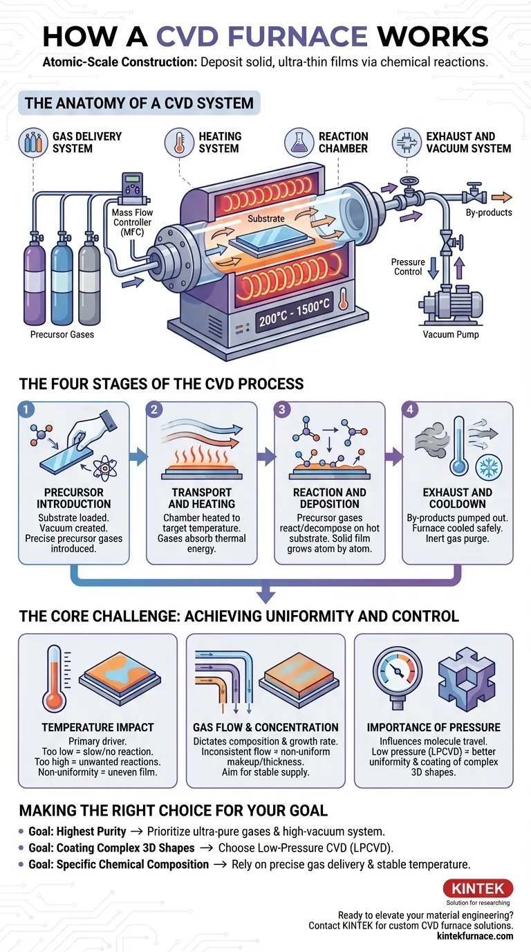
The Anatomy of a CVD System
To understand the process, you must first understand its essential components. A CVD furnace is a system where each part plays a critical role in controlling the deposition environment.
The Reaction Chamber
This is the heart of the furnace, typically a quartz tube or a stainless steel chamber. It houses the substrate and contains the chemical reaction. Its design is crucial for maintaining a clean, controlled atmosphere.
The Gas Delivery System
This system introduces one or more precursor gases into the chamber with extreme precision. It uses mass flow controllers (MFCs) to ensure the exact mixture and volume of gases are delivered at the correct time, which directly determines the composition of the final film.
The Heating System
Surrounding the reaction chamber, the heating system (e.g., resistance heaters or induction coils) raises the temperature to the target level, often between 200°C and 1500°C. Uniform heating across the substrate is paramount for creating a film of even thickness.
The Exhaust and Vacuum System
This system removes unreacted precursor gases and chemical by-products from the chamber. It also controls the chamber's pressure, allowing the process to run under high vacuum, low pressure, or at atmospheric pressure, depending on the specific requirements.
The Four Stages of the CVD Process
The deposition of a thin film via CVD is a sequential, four-step operation. Each stage must be executed flawlessly to achieve the desired result.
Stage 1: Precursor Introduction
The process begins by placing the substrate into the chamber and creating the desired atmosphere, often a vacuum. Then, carefully measured amounts of volatile precursor gases are introduced into the chamber via the gas delivery system.
Stage 2: Transport and Heating
The chamber is heated to a precise temperature. As the precursor gases flow over the hot substrate, they absorb thermal energy. This energy is the catalyst for the chemical reactions that will follow.
Stage 3: Reaction and Deposition
Once energized by the heat, the precursor gases react or decompose on or near the hot substrate surface. This chemical change "releases" the desired solid material, which deposits onto the substrate atom by atom, forming a thin, solid, and highly pure film. The properties of this film—its thickness, composition, and structure—are a direct result of the process conditions.
Stage 4: Exhaust and Cooldown
Throughout the process, gaseous by-products and any unreacted gases are continuously pumped out through the exhaust system. After the desired film thickness is achieved, the gas flow is stopped, and the furnace is safely cooled down. Purging with an inert gas prevents unwanted reactions or contamination during cooldown.
The Core Challenge: Achieving Uniformity and Control
The power of CVD lies in its precision, but this precision is dependent on managing several critical variables. A failure to control any one of these can compromise the entire process.
The Impact of Temperature
Temperature is the primary driver of the chemical reaction. If the temperature is too low, the reaction rate will be slow or nonexistent. If it is too high, unwanted gas-phase reactions can occur, leading to particle formation and poor film quality. Non-uniform heating leads directly to a film of non-uniform thickness.
The Role of Gas Flow and Concentration
The rate and ratio of precursor gases dictate the composition and growth rate of the film. Inconsistent flow can result in a film with a non-uniform chemical makeup or thickness. The goal is to provide a stable, consistent supply of reactants to the entire substrate surface.
The Importance of Pressure
Pressure influences the concentration of gas molecules and how they travel within the chamber. Low-pressure CVD (LPCVD) often results in better film uniformity and the ability to coat complex, three-dimensional shapes because the gas molecules can move more freely and reach all surfaces.
Making the Right Choice for Your Goal
The specific parameters of a CVD process are always tailored to the desired outcome. Understanding your primary objective is key to setting up the process correctly.
- If your primary focus is the highest possible purity: Prioritize ultra-pure precursor gases and a high-vacuum system to eliminate contaminants.
- If your primary focus is coating complex, 3D shapes: A low-pressure CVD (LPCVD) process is superior, as it promotes uniform deposition across all exposed surfaces.
- If your primary focus is achieving a specific chemical composition: Your success depends entirely on the precision of your gas delivery system and maintaining stable temperature control.
By mastering these fundamental principles, you can effectively use a CVD furnace to engineer materials with precision, one atomic layer at a time.
Summary Table:
| Component/Stage | Key Function |
|---|---|
| Reaction Chamber | Houses substrate and reaction, maintains controlled atmosphere |
| Gas Delivery System | Introduces precise precursor gases via mass flow controllers |
| Heating System | Heats chamber uniformly (200°C-1500°C) to drive reactions |
| Exhaust and Vacuum System | Removes by-products, controls pressure for uniformity |
| Stage 1: Precursor Introduction | Places substrate, creates vacuum, introduces gases |
| Stage 2: Transport and Heating | Heats chamber, gases absorb thermal energy |
| Stage 3: Reaction and Deposition | Gases react/decompose, deposit solid film atom by atom |
| Stage 4: Exhaust and Cooldown | Pumps out gases, cools furnace, purges with inert gas |
Ready to elevate your material engineering with a custom CVD furnace? At KINTEK, we leverage exceptional R&D and in-house manufacturing to provide advanced high-temperature furnace solutions tailored for diverse laboratories. Our product line includes CVD/PECVD Systems, Muffle, Tube, Rotary, Vacuum, and Atmosphere Furnaces, all backed by strong deep customization capabilities to precisely meet your unique experimental needs—whether you're focused on high purity, coating complex 3D shapes, or specific chemical compositions. Contact us today to discuss how we can help you achieve superior thin-film deposition and optimize your research outcomes!
Visual Guide
Related Products
- Custom Made Versatile CVD Tube Furnace Chemical Vapor Deposition CVD Equipment Machine
- Split Chamber CVD Tube Furnace with Vacuum Station CVD Machine
- Multi Heating Zones CVD Tube Furnace Machine for Chemical Vapor Deposition Equipment
- Slide PECVD Tube Furnace with Liquid Gasifier PECVD Machine
- Controlled Inert Nitrogen Hydrogen Atmosphere Furnace
People Also Ask
- How can integrating CVD tube furnaces with other technologies benefit device fabrication? Unlock Advanced Hybrid Processes
- What are the practical applications of gate media prepared by CVD tube furnaces? Unlock Advanced Electronics and More
- What customization options are available for CVD tube furnaces? Tailor Your System for Superior Material Synthesis
- Which industries and research fields benefit from CVD tube furnace sintering systems for 2D materials? Unlock Next-Gen Tech Innovations
- What are the key features of CVD tube furnaces for 2D material processing? Unlock Precision Synthesis for Superior Materials


