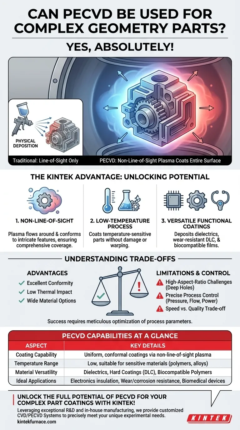
Yes, absolutely. Plasma-Enhanced Chemical Vapor Deposition (PECVD) is a highly effective method for applying uniform coatings to parts with complex geometries. Unlike line-of-sight deposition techniques, PECVD uses an energized gas, or plasma, that can flow around and conform to intricate features, ensuring comprehensive surface coverage.
The key advantage of PECVD is not just its ability to coat complex shapes, but its power to do so at low temperatures with a wide range of high-performance materials. Success depends on understanding that achieving perfect uniformity on intricate surfaces is a matter of precise process control, not an automatic guarantee.
How PECVD Coats Complex Geometries
PECVD’s unique capabilities stem from its fundamental mechanism, which is distinct from physical deposition methods that act like a spray gun.
The Power of Non-Line-of-Sight Deposition
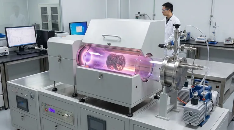
PECVD is a non-line-of-sight process. Instead of physically sputtering a target, it introduces precursor gases into a vacuum chamber and energizes them into a plasma.
This reactive plasma envelops the entire part, regardless of its orientation. The chemical reactions that form the coating happen directly on all exposed surfaces, allowing the film to "grow" conformally over curves, into channels, and around sharp corners.
Lower Temperatures Protect Sensitive Parts
A defining feature of PECVD is its relatively low operating temperature compared to traditional Chemical Vapor Deposition (CVD).
This makes it possible to coat temperature-sensitive materials, such as polymers or certain metal alloys, without causing thermal damage or warping. Complex parts, especially in biomedical or electronics fields, are often made from such materials.
Versatility in Functional Coatings
The ability to coat a complex shape is only useful if the coating provides a necessary function. PECVD excels at depositing a diverse range of materials.
This includes dielectrics like silicon dioxide (SiO2) and silicon nitride (Si3N4) for electrical insulation, hard coatings like Diamond-like Carbon (DLC) for wear resistance, and specialized polymers for creating biocompatible or corrosion-resistant surfaces.
Understanding the Trade-offs
While powerful, PECVD is not a magic bullet. Achieving a high-quality, uniform coating on a complex part requires careful consideration of the process limitations.
Conformality Has Its Limits
While PECVD is excellent for general conformity, extremely high-aspect-ratio features (very deep, narrow holes or trenches) can be challenging.
The precursor gases can become depleted before they reach the bottom of these features, or the plasma density may vary, leading to a thinner coating at the base than at the top. This is a factor of gas transport and plasma physics.
Process Control is Non-Negotiable
Achieving a truly uniform coating on a complex surface requires meticulous optimization.
Factors like chamber pressure, gas flow rates, RF power, and even the placement of the part within the chamber must be precisely controlled. What works for a flat wafer will not work for a multi-faceted mechanical component without significant process development.
Deposition Rate vs. Film Quality
There is often a trade-off between the speed of deposition and the quality of the resulting film.
Attempting to coat a part too quickly can lead to a less dense, more porous film with poorer adhesion, especially on challenging geometries. Slower, more controlled deposition generally yields a higher-quality, more uniform coating.
Making the Right Choice for Your Goal
To determine if PECVD is the right solution, you must match its capabilities to your specific technical requirements.
- If your primary focus is electrical insulation: PECVD is a superior choice for conformally coating intricate electronic components or sensors with high-quality dielectrics like SiO2.
- If your primary focus is wear or corrosion resistance: The technique is ideal for applying hard DLC or inert ceramic films onto mechanical parts like gears, molds, or medical implants.
- If your primary focus is a biocompatible surface on a polymer device: PECVD's low-temperature process is one of the few methods that can deposit functional coatings onto complex polymer-based medical devices without damaging the substrate.
Ultimately, PECVD's strength lies in its ability to combine functional material deposition with excellent conformity for even the most challenging part designs.
Summary Table:
| Aspect | Key Details |
|---|---|
| Coating Capability | Uniform, conformal coatings on complex geometries via non-line-of-sight plasma process |
| Temperature Range | Low operating temperatures, suitable for sensitive materials like polymers and alloys |
| Material Versatility | Deposits dielectrics (e.g., SiO2), hard coatings (e.g., DLC), and biocompatible polymers |
| Key Advantages | Excellent surface coverage, low thermal impact, wide material options |
| Limitations | Challenges with high-aspect-ratio features; requires precise process control for uniformity |
| Ideal Applications | Electronics insulation, wear/corrosion resistance, biomedical device coatings |
Unlock the full potential of PECVD for your complex part coatings with KINTEK! Leveraging exceptional R&D and in-house manufacturing, we provide advanced high-temperature furnace solutions, including our specialized CVD/PECVD Systems. Our strong deep customization capability ensures we precisely meet your unique experimental needs, whether for electronics, biomedical devices, or industrial components. Contact us today to discuss how our tailored PECVD solutions can enhance your coating processes and drive innovation in your lab!
Visual Guide
Related Products
- Slide PECVD Tube Furnace with Liquid Gasifier PECVD Machine
- RF PECVD System Radio Frequency Plasma Enhanced Chemical Vapor Deposition
- Inclined Rotary Plasma Enhanced Chemical Deposition PECVD Tube Furnace Machine
- Inclined Rotary Plasma Enhanced Chemical Deposition PECVD Tube Furnace Machine
- Multi Heating Zones CVD Tube Furnace Machine for Chemical Vapor Deposition Equipment
People Also Ask
- What plasma source is used in PE-CVD tube furnaces? Unlock Low-Temperature, High-Quality Deposition
- In which industries is the tube furnace commonly used? Essential for Materials Science, Energy, and More
- What role does a Tube Furnace play in the CVD growth of carbon nanotubes? Achieve High-Purity CNT Synthesis
- What is plasma in the context of PECVD? Unlock Low-Temperature Thin Film Deposition
- What are the advantages of using a tube furnace CVD system for Cu(111)/graphene? Superior Scalability and Quality


