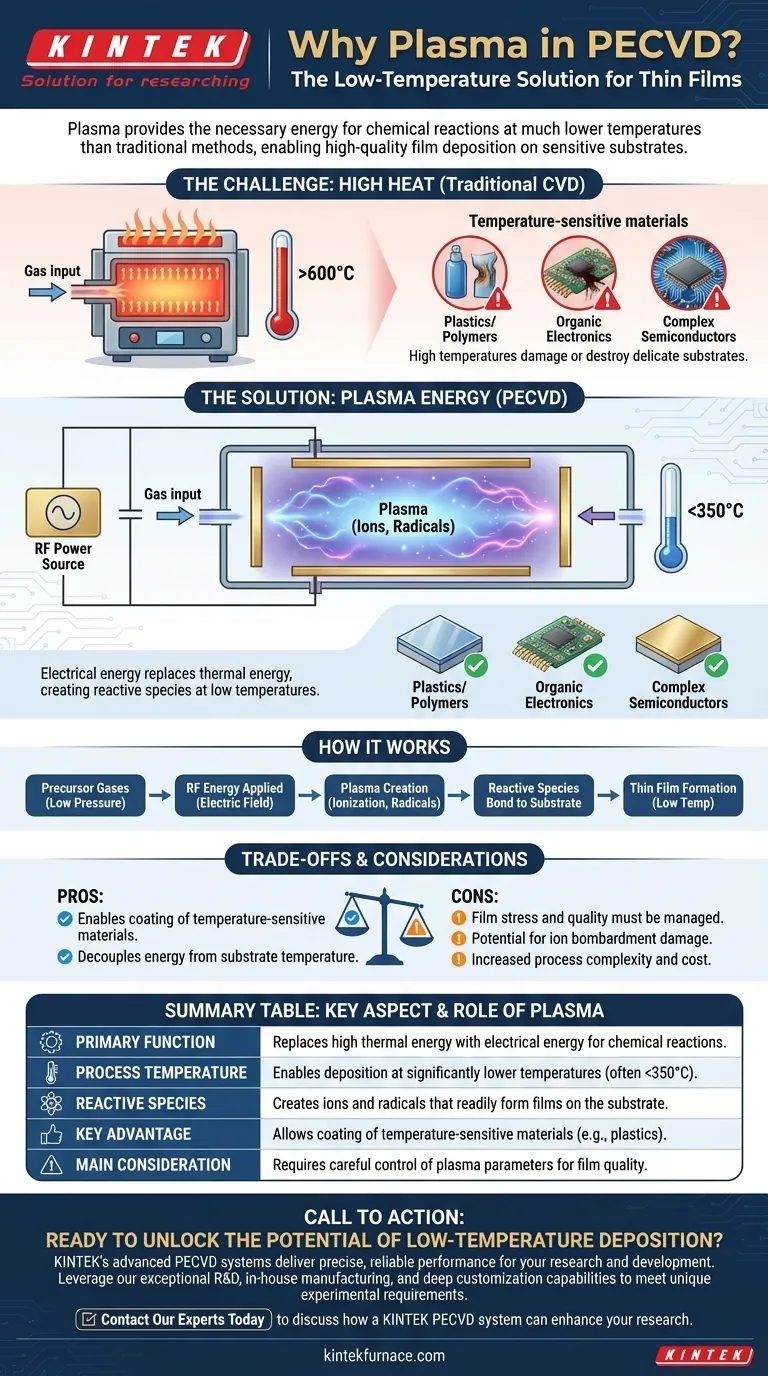
In short, plasma is used in Plasma-Enhanced Chemical Vapor Deposition (PECVD) to provide the necessary energy for chemical reactions at much lower temperatures than traditional methods. By ionizing precursor gases into a reactive plasma state, PECVD can deposit high-quality thin films onto substrates that would be damaged or destroyed by the high heat required for conventional thermal processes.
The core function of plasma in PECVD is to replace high thermal energy with electrical energy. This creates a low-temperature environment filled with highly reactive chemical species, enabling film deposition without subjecting the substrate to damaging heat.
The Fundamental Challenge: Energy for Deposition
To understand the value of plasma, we must first understand the basic requirement of any Chemical Vapor Deposition (CVD) process: energy.
The Traditional Approach: Thermal Energy
In conventional CVD, precursor gases are introduced into a high-temperature furnace. The intense heat provides the thermal energy needed to break the chemical bonds within these gas molecules.
The resulting atoms or smaller molecules then deposit onto the substrate, gradually building up the desired thin film. This process is effective but requires very high temperatures, often several hundred degrees Celsius.
The Problem with High Heat
High processing temperatures are a significant limitation. They make it impossible to deposit films on temperature-sensitive materials like plastics, organic electronics, or complex semiconductor devices that already have delicate, low-melting-point structures. The heat would simply warp, melt, or destroy the substrate.
Plasma: The Low-Temperature Solution
PECVD was developed specifically to overcome this temperature barrier. It achieves this by changing the very nature of the energy source.
What is Plasma?
Plasma is often called the fourth state of matter. It is a gas in which a significant portion of the atoms or molecules have been ionized by an electric field, creating a mixture of ions, electrons, and highly reactive neutral species called radicals.
How Plasma Replaces Heat
In a PECVD reactor, a low-pressure gas is energized by applying a voltage between two electrodes, typically using a radio frequency (RF) power source. This electric field, not high heat, provides the energy.
This energy strips electrons from the gas molecules, instantly creating the reactive plasma. The energy is transferred directly to the gas molecules, bypassing the need to heat the entire chamber and substrate.
The Role of Reactive Species
The ions and radicals within the plasma are chemically unstable and extremely reactive. When they come into contact with the substrate surface, they readily react and bond to form a stable, solid thin film.
Because their high reactivity comes from their electronic state rather than thermal energy, this entire process can occur at much lower substrate temperatures, often below 350°C.
Understanding the Trade-offs
While revolutionary, using plasma is not without its considerations. An objective analysis requires understanding the trade-offs involved.
Film Quality and Stress
Films deposited via PECVD can have different properties, such as density and internal stress, compared to those grown at high temperatures. These properties must be carefully managed through process parameter tuning to meet application requirements.
Potential for Ion Bombardment
The energetic ions within the plasma can physically bombard the growing film. While this can sometimes be beneficial for densifying the film, excessive bombardment can introduce defects or damage the substrate surface. Controlling plasma energy is critical.
Process Complexity
PECVD systems are inherently more complex than simple thermal CVD furnaces. They require sophisticated vacuum systems, precise gas flow controllers, and stable RF power delivery systems, which can increase equipment and operational costs.
Making the Right Choice for Your Application
Your choice between PECVD and other methods depends entirely on the constraints and goals of your project.
- If your primary focus is depositing on temperature-sensitive substrates: PECVD is the clear and often only viable choice.
- If your primary focus is achieving the highest possible film purity and crystallinity: High-temperature thermal CVD may still be superior, provided the substrate can withstand the heat.
- If your primary focus is balancing film quality with high throughput on robust substrates: PECVD offers an excellent, highly tunable process for many industrial applications.
Ultimately, PECVD empowers engineers and scientists by decoupling the energy required for deposition from the temperature of the substrate.
Summary Table:
| Key Aspect | Role of Plasma in PECVD |
|---|---|
| Primary Function | Replaces high thermal energy with electrical energy for chemical reactions. |
| Process Temperature | Enables deposition at significantly lower temperatures (often <350°C). |
| Reactive Species | Creates ions and radicals that readily form films on the substrate. |
| Key Advantage | Allows coating of temperature-sensitive materials (e.g., plastics, advanced semiconductors). |
| Main Consideration | Requires careful control of plasma parameters to manage film stress and quality. |
Ready to unlock the potential of low-temperature thin film deposition for your sensitive substrates?
KINTEK's advanced PECVD systems are engineered to deliver precise, reliable performance. Leveraging our exceptional R&D and in-house manufacturing, we provide robust solutions for diverse laboratory needs. Our product line, including PECVD Systems, is complemented by strong deep customization capabilities to precisely meet your unique experimental requirements.
Contact our experts today to discuss how a KINTEK PECVD system can enhance your research and development.
Visual Guide
Related Products
- Slide PECVD Tube Furnace with Liquid Gasifier PECVD Machine
- RF PECVD System Radio Frequency Plasma Enhanced Chemical Vapor Deposition
- Inclined Rotary Plasma Enhanced Chemical Deposition PECVD Tube Furnace Machine
- Inclined Rotary Plasma Enhanced Chemical Deposition PECVD Tube Furnace Machine
- Multi Heating Zones CVD Tube Furnace Machine for Chemical Vapor Deposition Equipment
People Also Ask
- What role does a Tube Furnace play in the CVD growth of carbon nanotubes? Achieve High-Purity CNT Synthesis
- How does PECVD equipment contribute to TOPCon bottom cells? Mastering Hydrogenation for Maximum Solar Efficiency
- What are the main advantages of PECVD tube furnaces compared to CVD tube furnaces? Lower Temp, Faster Deposition, and More
- What are the disadvantages of tube furnace cracking when processing heavy raw materials? Avoid Costly Downtime and Inefficiency
- How does a hydrogen reduction environment in an industrial tube furnace facilitate gold-copper alloy microspheres?


