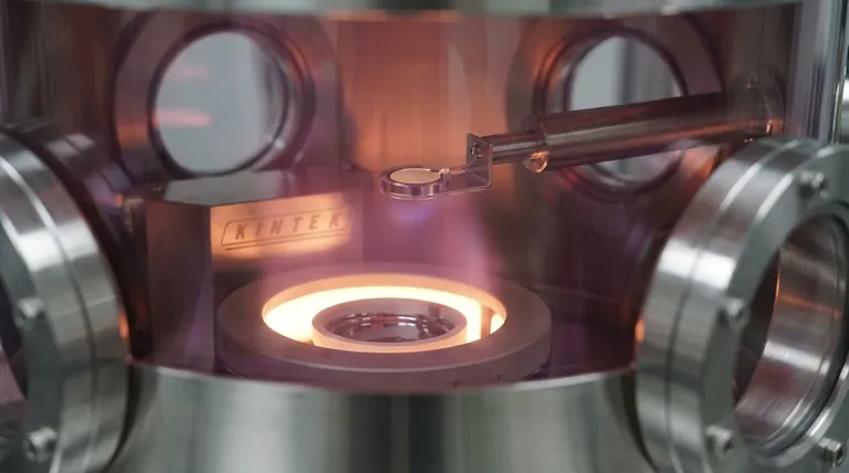
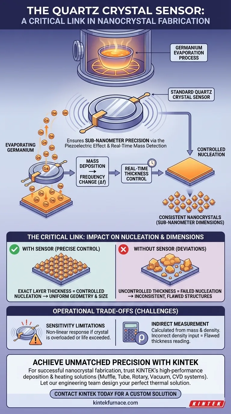
A standard Quartz Crystal Sensor is the primary mechanism for ensuring sub-nanometer precision during the germanium evaporation process. By leveraging the piezoelectric effect, this device detects minute changes in deposited mass in real-time. This capability allows for exact control over the thickness of the evaporated layer, which is the foundational variable in defining the final properties of the nanocrystals.
In nanocrystal fabrication, the thickness of the deposited material directly dictates the nucleation process. The Quartz Crystal Sensor acts as the critical feedback loop, translating mass changes into precise thickness measurements to ensure the dimensions of the final product meet strict specifications.
The Mechanics of Precision Control
Utilizing the Piezoelectric Effect
The sensor operates by exploiting the piezoelectric effect. This physical phenomenon allows the sensor to translate mechanical stress—in this case, the weight of the depositing material—into a measurable electrical signal.
Real-Time Mass Detection
As germanium evaporates and lands on the sensor, the added mass alters the crystal's oscillation frequency.
Because this detection happens in real-time, engineers can monitor the rate of deposition instantly. This prevents the need for post-process measurements, which are often too late to correct errors.
The Critical Link to Nanocrystal Formation
Impact on Nucleation
The primary reference indicates that the fabrication of nanocrystals is highly sensitive to the initial layer thickness.
Even minor deviations in the amount of germanium deposited can fundamentally alter the nucleation process. Nucleation is the "seed" stage where the crystal begins to form; if this stage is uncontrolled, the entire structure may fail.
Achieving Sub-Nanometer Dimensions
To achieve specific nanocrystal dimensions, the margin for error is virtually non-existent.
The Quartz Crystal Sensor provides sub-nanometer precision, ensuring that the evaporated layer is exactly as thick as required to support the desired crystal geometry. Without this level of granularity, achieving consistent nanocrystal sizes is impossible.
Understanding the Operational Trade-offs
Sensitivity Limitations
While the sensor provides high precision, it relies entirely on the accuracy of the mass detection. If the sensor becomes overloaded or the "crystal life" is exceeded, the frequency response may become non-linear, leading to inaccurate thickness readings.
Indirect Measurement
It is important to remember that the sensor measures mass, not physical thickness directly.
The system calculates thickness based on the density of germanium. If the density parameters entered into the controller are incorrect, or if the material density changes during deposition, the resulting thickness reading will be flawed despite the sensor working correctly.
Ensuring Process Integrity
To maximize the effectiveness of the Quartz Crystal Sensor in your fabrication workflow, consider the following focus areas:
- If your primary focus is Dimensional Uniformity: Rely on the sensor’s sub-nanometer precision to maintain strict consistency across different fabrication runs.
- If your primary focus is Process Stability: Monitor the real-time feedback loop to instantly identify and correct any deviations in the evaporation rate before they affect nucleation.
Precise control of the germanium layer is the single most important factor in transitioning from raw material to functional nanocrystal.
Summary Table:
| Feature | Function in Germanium Evaporation | Impact on Nanocrystals |
|---|---|---|
| Piezoelectric Effect | Translates mass changes into electrical signals | Enables sub-nanometer thickness control |
| Real-Time Monitoring | Detects mass deposition during evaporation | Allows immediate adjustments to nucleation |
| Frequency Response | Measures oscillation changes | Ensures consistent crystal geometry and size |
| Feedback Loop | Provides continuous rate data | Prevents deviations in structural integrity |
Achieve Unmatched Precision in Your Nanotechnology Research
Precision is the difference between a successful experiment and a failed nucleation process. KINTEK provides the high-performance deposition and heating environments necessary for advanced nanocrystal fabrication. Backed by expert R&D and manufacturing, we offer a comprehensive range of Muffle, Tube, Rotary, Vacuum, and CVD systems, all customizable to meet your specific germanium evaporation and material science requirements.
Don't let minor deviations compromise your results. Let our engineering team help you design the perfect thermal solution for your lab.
Contact KINTEK Today for a Custom Solution
Visual Guide
References
- Z. Remeš, Oleg Babčenko. Thin Hydrogenated Amorphous Silicon Carbide Layers with Embedded Ge Nanocrystals. DOI: 10.3390/nano15030176
This article is also based on technical information from Kintek Furnace Knowledge Base .
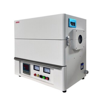
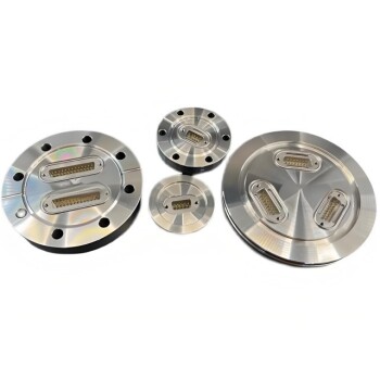
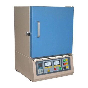
Related Products
- Ultra High Vacuum Observation Window Stainless Steel Flange Sapphire Glass Sight Glass for KF
- Multi Zone Laboratory Quartz Tube Furnace Tubular Furnace
- Laboratory Quartz Tube Furnace RTP Heating Tubular Furnace
- Ultra High Vacuum CF Flange Stainless Steel Sapphire Glass Observation Sight Window
- Ultra High Vacuum CF Observation Window Flange with High Borosilicate Glass Sight Glass
People Also Ask
- Why is an environmental laboratory chamber equipped with an optical window required for synthesizing Hafnium Carbide?
- What is the purpose of utilizing a glassy carbon crucible and HCl gas treatment? Ensure Pure Molten Salt Systems
- What are the advantages of 0.7 mm quartz capillaries for SXRD? Optimize High-Energy In-Situ X-ray Experiments
- What is the core function of a high-purity quartz crucible? Ensuring Success in Czochralski Silicon Growth
- Why is an Ultra-High Vacuum (UHV) System Required for In2Se3? Achieving Atomic-Level Ferroelectric Clarity