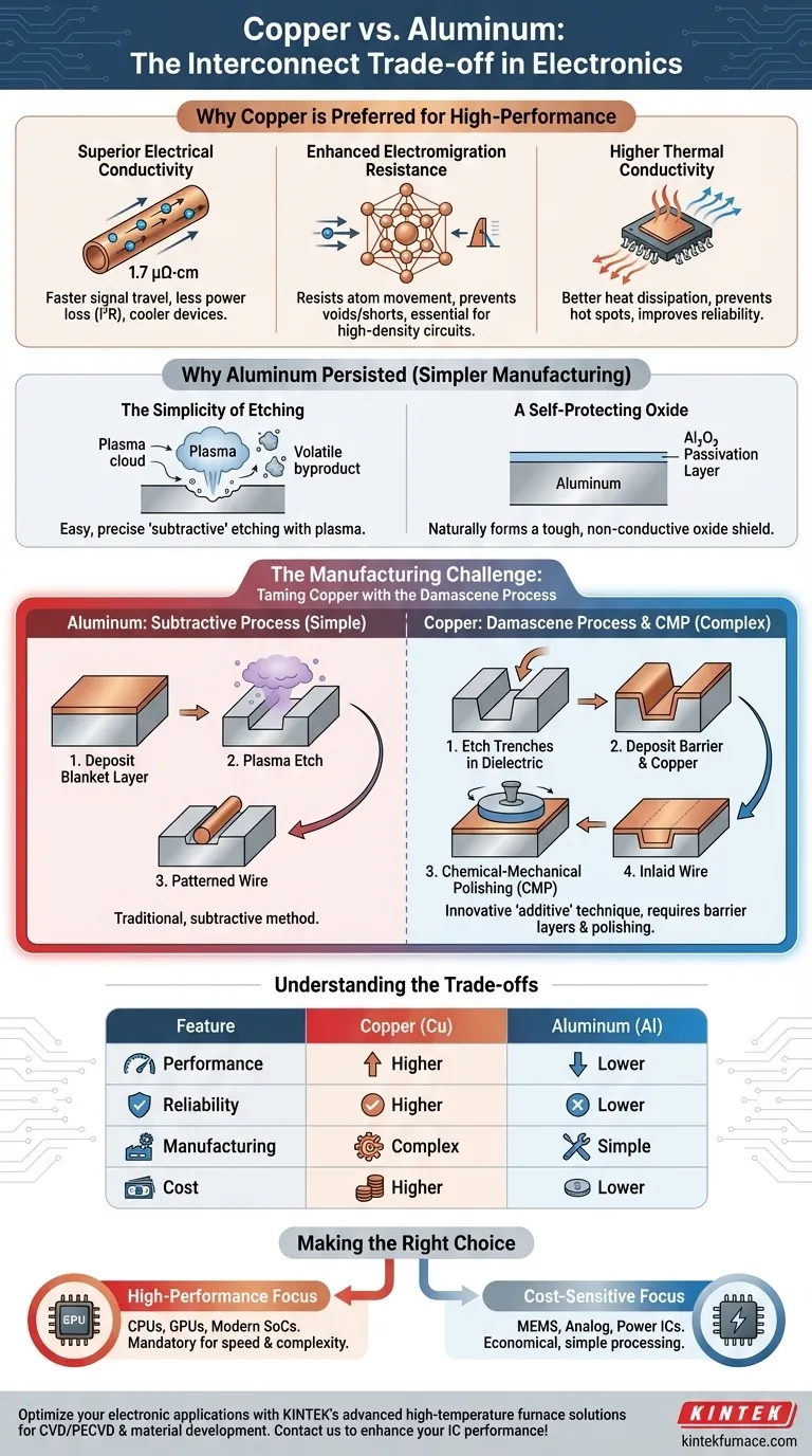
In modern electronics, copper films are decisively preferred over aluminum for high-performance applications primarily due to their superior electrical conductivity and significantly higher resistance to electromigration. This allows for the creation of faster, more power-efficient, and more reliable integrated circuits (ICs) with denser wiring.
The choice between copper and aluminum is not merely about picking the best conductor; it is a fundamental engineering trade-off. Copper offers superior electrical performance and longevity, but at the cost of significantly more complex and expensive manufacturing processes compared to the established, simpler methods used for aluminum.
The Core Advantages of Copper Interconnects
For decades, aluminum was the standard for the metal wiring layers (interconnects) that connect transistors on a chip. The shift to copper, which began in the late 1990s, was a critical inflection point in semiconductor manufacturing driven by clear performance imperatives.
Superior Electrical Conductivity
Copper's most well-known advantage is its lower electrical resistivity (around 1.7 µΩ·cm) compared to aluminum (around 2.7 µΩ·cm).
This lower resistance directly translates to less signal delay, allowing electrical signals to travel faster through the chip's wiring. It also reduces resistive power loss (I²R loss), meaning less energy is wasted as heat, leading to more power-efficient and cooler-running devices.
Enhanced Electromigration Resistance
Electromigration is the gradual movement of metal atoms in a conductor caused by the "push" from flowing electrons. Over time, this can create voids that lead to open circuits or hillocks that cause short circuits, ultimately causing the chip to fail.
Copper atoms are heavier and have a higher melting point, making them substantially more resistant to electromigration than aluminum atoms. This increased durability is essential for modern, high-density circuits where wires are incredibly thin and carry high current densities.
Higher Thermal Conductivity
Copper is also a better thermal conductor than aluminum. It is more efficient at dissipating the heat it generates, preventing the formation of localized hot spots on the chip.
This property works in concert with its lower electrical resistance to improve the overall thermal management and reliability of the device.
Why Aluminum Persisted (And Still Has a Place)
If copper is superior, the logical question is why aluminum was used for so long. The answer lies not in performance, but in manufacturability.
The Simplicity of Etching
The traditional method for patterning wires on a chip is a "subtractive" process: deposit a blanket layer of metal, then use a plasma etching process to remove the unwanted material.
Aluminum reacts readily in chlorine- or fluorine-based plasmas to form volatile byproducts, making it very easy to etch with high precision. This made manufacturing simple and cost-effective.
A Self-Protecting Oxide
Aluminum naturally and instantly forms a thin, tough, and non-conductive layer of aluminum oxide (Al₂O₃) upon exposure to air. This "passivation" layer protects the underlying metal from corrosion and acts as an excellent adhesion surface for the insulating dielectric materials layered on top of it.
The Manufacturing Challenge: Taming Copper
The primary obstacle to adopting copper was that it is extremely difficult to etch using plasma. It does not form volatile compounds under typical etching conditions, so the subtractive method used for aluminum simply does not work.
The Damascene Process Solution
The industry solved this by inventing an entirely new "additive" manufacturing technique called the Damascene process.
Instead of etching the metal itself, trenches and vias (vertical connections) are first etched into the insulating silicon dioxide layer where the wires are intended to be.
Deposition and Polishing
Next, a thin barrier layer (often tantalum/tantalum nitride) is deposited to prevent copper from diffusing into the silicon, which would poison the transistors. Then, a blanket layer of copper is deposited over the entire wafer, completely filling the trenches.
Finally, a process called Chemical-Mechanical Polishing (CMP) is used to polish and grind away the excess copper from the surface, leaving the metal only "inlaid" within the predefined trenches. This revolutionary technique was the key that unlocked copper's use in ICs.
Understanding the Trade-offs
The decision to use copper or aluminum is a clear case of balancing performance against complexity and cost.
| Feature | Copper (Cu) | Aluminum (Al) |
|---|---|---|
| Performance | Higher. Lower resistance and signal delay. | Lower. Higher resistance and power loss. |
| Reliability | Higher. Excellent electromigration resistance. | Lower. Prone to electromigration failure. |
| Manufacturing | Complex. Requires Damascene/CMP and barrier layers. | Simple. Uses established subtractive etching. |
| Material Cost | Higher. | Lower. |
Making the Right Choice for Your Application
Ultimately, the material choice is dictated entirely by the application's specific requirements.
- If your primary focus is maximum performance and density (CPUs, GPUs, modern SoCs): Copper is the mandatory choice. Its superior conductivity and reliability are essential for enabling the speed and complexity of advanced logic devices.
- If your primary focus is cost-sensitivity or specific applications (some power ICs, MEMS, analog circuits): Aluminum remains a perfectly viable and economical option where its performance limitations are acceptable and its simple processing is a major advantage.
- If your primary focus is chip packaging (wire bonding): Aluminum is still heavily favored for the top-layer bond pads, as its stable native oxide provides a reliable surface for attaching the gold or aluminum wires that connect the chip to its package.
Understanding these fundamental material trade-offs empowers you to select the interconnect strategy that truly aligns with your project's performance, cost, and reliability goals.
Summary Table:
| Feature | Copper (Cu) | Aluminum (Al) |
|---|---|---|
| Electrical Conductivity | Higher (1.7 µΩ·cm) | Lower (2.7 µΩ·cm) |
| Electromigration Resistance | Excellent | Poor |
| Thermal Conductivity | Higher | Lower |
| Manufacturing Complexity | High (Damascene/CMP) | Low (Subtractive Etching) |
| Cost | Higher | Lower |
| Ideal Applications | High-performance ICs, CPUs, GPUs | Cost-sensitive ICs, MEMS, Analog Circuits |
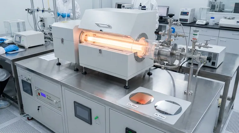
Optimize your electronic applications with KINTEK's advanced high-temperature furnace solutions! Leveraging exceptional R&D and in-house manufacturing, we provide diverse laboratories with products like Muffle, Tube, Rotary Furnaces, Vacuum & Atmosphere Furnaces, and CVD/PECVD Systems. Our strong deep customization capability ensures we precisely meet your unique experimental requirements for developing reliable copper or aluminum films. Contact us today to enhance your IC performance and efficiency!
Visual Guide
Related Products
- Custom Made Versatile CVD Tube Furnace Chemical Vapor Deposition CVD Equipment Machine
- Multi Heating Zones CVD Tube Furnace Machine for Chemical Vapor Deposition Equipment
- HFCVD Machine System Equipment for Drawing Die Nano Diamond Coating
- Slide PECVD Tube Furnace with Liquid Gasifier PECVD Machine
- Inclined Rotary Plasma Enhanced Chemical Deposition PECVD Tube Furnace Machine
People Also Ask
- What are the practical applications of gate media prepared by CVD tube furnaces? Unlock Advanced Electronics and More
- What temperature range do standard CVD tube furnaces operate at? Unlock Precision for Your Material Deposition
- What are the key features of CVD tube furnaces for 2D material processing? Unlock Precision Synthesis for Superior Materials
- What are the benefits of developing new precursor materials for CVD tube furnaces? Unlock Advanced Thin-Film Synthesis
- What is a CVD tube furnace and what is its primary function? Discover Precision Thin-Film Deposition