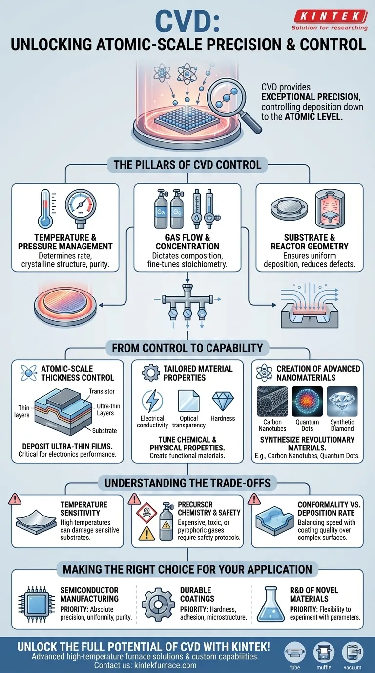
In short, Chemical Vapor Deposition (CVD) provides an exceptionally high level of precision, allowing for control down to the atomic level. This is achieved by meticulously managing the core process parameters—temperature, pressure, and gas composition—which directly dictate the structure and properties of the final material.
The true value of CVD lies not just in its precision, but in how that precision translates into capability. By controlling the deposition environment, you gain the power to engineer materials with specific, tailored properties that are impossible to achieve through other methods.
The Pillars of CVD Control
The precision of CVD is not a single feature but the result of controlling several interdependent variables. Understanding these pillars is key to leveraging the process effectively.
Temperature and Pressure Management
The temperature of the substrate and the pressure within the reaction chamber are the primary drivers of the chemical reaction. Precise control over these factors determines the rate of deposition, the crystalline structure of the film, and its overall quality and purity.
Gas Flow and Concentration
CVD works by introducing precursor gases into a chamber. The flow rate and concentration of these gases dictate the chemical composition of the deposited film. This allows for the creation of complex compound materials and the ability to fine-tune stoichiometry with remarkable accuracy.
Substrate and Reactor Geometry
The physical setup, including the shape of the substrate and the design of the reactor, also plays a critical role. These elements influence the flow dynamics of the gases, ensuring the precursor chemicals are delivered uniformly across the substrate surface. This control is essential for producing consistent, defect-free films over large areas.
From Control to Capability: What This Precision Unlocks
This fine-grained control is not just an academic exercise; it directly enables the production of today's most advanced materials and devices.
Atomic-Scale Thickness Control
The most significant advantage of CVD is the ability to deposit ultra-thin films, often just a few atomic layers thick. This is fundamental to modern electronics, where the performance of a transistor can be determined by the thickness and perfection of a single, nanometer-scale layer.
Tailored Material Properties
By adjusting the deposition parameters, you can precisely tune the chemical and physical properties of the material. This includes everything from its electrical conductivity and optical transparency to its hardness and chemical resistance, allowing a single process to create a wide variety of functional materials.
Creation of Advanced Nanomaterials
This level of control is instrumental in synthesizing revolutionary materials. For example, CVD is a primary method for growing carbon nanotubes for next-generation electronics, creating quantum dots for medical imaging, and producing high-purity synthetic diamond films for industrial tools and optics.
Understanding the Trade-offs
While powerful, CVD is not without its operational complexities and limitations. Acknowledging these is crucial for successful implementation.
Temperature Sensitivity
Many CVD processes require very high temperatures, which can damage or warp temperature-sensitive substrates. This limits the types of materials that can be coated and often requires specialized equipment or alternative, lower-temperature CVD techniques (like PECVD).
Precursor Chemistry and Safety
The precursor gases used in CVD can be expensive, highly toxic, or pyrophoric (igniting spontaneously in air). Managing these materials requires significant investment in safety infrastructure and handling protocols, adding to the overall cost and complexity of the process.
Conformality vs. Deposition Rate
Achieving a perfectly uniform coating over a complex, three-dimensional surface (high conformality) often requires slower deposition rates. There is a constant trade-off between the speed of the process and the quality and uniformity of the resulting film, which must be optimized for each specific application.
Making the Right Choice for Your Application
Your specific goal will determine which aspects of CVD's control are most critical.
- If your primary focus is semiconductor manufacturing: Your priority is absolute precision in film thickness, uniformity, and purity, demanding tight control over all process parameters.
- If your primary focus is creating durable coatings: Your concern is optimizing for hardness and adhesion, which means focusing on temperature and precursor choice to control the film's microstructure.
- If your primary focus is research and development of novel materials: The flexibility to experiment with a wide range of gas concentrations, flow rates, and temperatures is your most valuable asset.
Ultimately, mastering CVD is about understanding how to translate a set of controlled inputs into a desired material outcome.
Summary Table:
| Aspect of Control | Key Parameters | Impact on Material |
|---|---|---|
| Temperature & Pressure | Substrate temp, chamber pressure | Determines deposition rate, crystalline structure, purity |
| Gas Flow & Concentration | Flow rate, gas composition | Controls film stoichiometry, enables complex compounds |
| Substrate & Reactor Geometry | Shape, reactor design | Ensures uniform deposition, reduces defects |
| Atomic-Scale Thickness | Precise layer control | Essential for ultra-thin films in electronics |
| Tailored Properties | Parameter adjustments | Tunes electrical, optical, and mechanical traits |
Unlock the full potential of CVD for your laboratory with KINTEK! Leveraging exceptional R&D and in-house manufacturing, we provide advanced high-temperature furnace solutions like CVD/PECVD Systems, Muffle, Tube, Rotary, Vacuum & Atmosphere Furnaces. Our strong deep customization capability ensures precise alignment with your unique experimental needs, whether for semiconductor production, durable coatings, or novel material R&D. Contact us today to discuss how our tailored solutions can enhance your precision and efficiency!
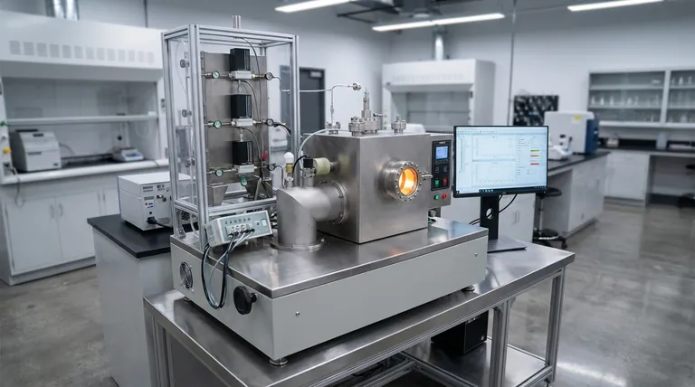
Visual Guide
Related Products
- Custom Made Versatile CVD Tube Furnace Chemical Vapor Deposition CVD Equipment Machine
- Multi Heating Zones CVD Tube Furnace Machine for Chemical Vapor Deposition Equipment
- HFCVD Machine System Equipment for Drawing Die Nano Diamond Coating
- Split Chamber CVD Tube Furnace with Vacuum Station CVD Machine
- 915MHz MPCVD Diamond Machine Microwave Plasma Chemical Vapor Deposition System Reactor
People Also Ask
- What future trends are expected in the development of CVD tube furnaces? Discover Smarter, More Versatile Systems
- What is a CVD tube furnace and what is its primary function? Discover Precision Thin-Film Deposition
- What improvements can be made to the bonding force of gate dielectric films using a CVD tube furnace? Enhance Adhesion for Reliable Devices
- Why are CVD tube furnace sintering systems indispensable for 2D material research and production? Unlock Atomic-Scale Precision
- How does CVD tube furnace sintering enhance graphene growth? Achieve Superior Crystallinity and High Electron Mobility


