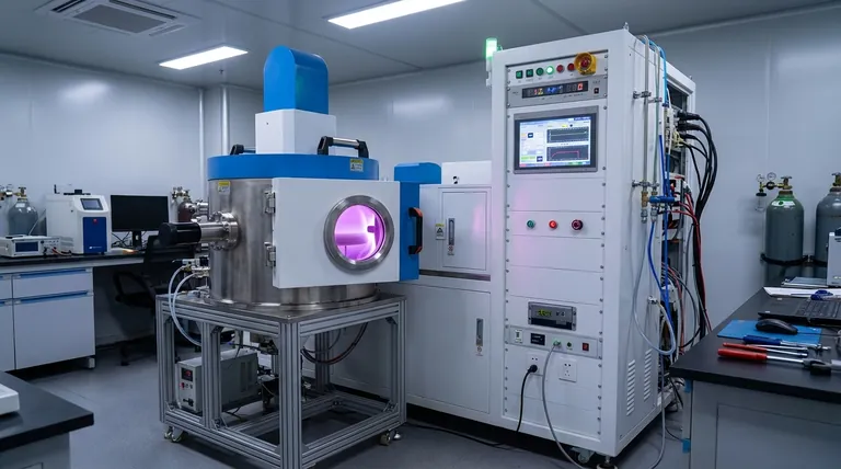
In essence, a plasma deposition system is a highly specialized machine that uses an energized gas, known as plasma, to synthesize and deposit ultra-thin films of material onto a surface. Unlike simple coating methods, these systems facilitate chemical reactions in a vacuum chamber, allowing for the creation of advanced materials with precisely controlled properties, ranging from synthetic diamonds to specialized polymer layers.
A plasma deposition system's core function is not merely to coat a surface, but to grow a new material layer atom-by-atom from a gas phase. It enables the creation of high-performance films at low temperatures that would be impossible to produce with conventional melting or coating techniques.
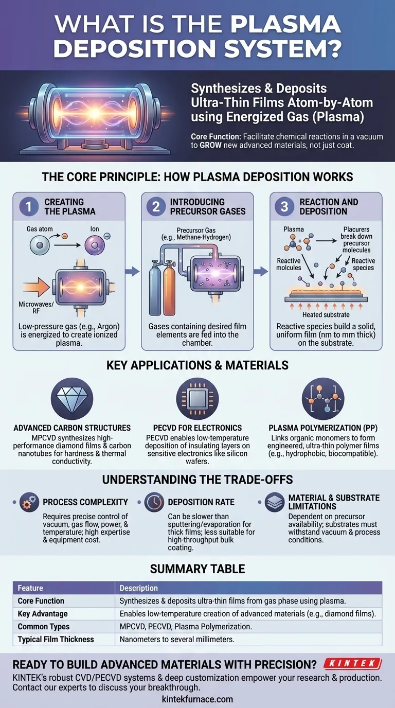
The Core Principle: How Plasma Deposition Works
At its heart, plasma deposition is a process of controlled material synthesis. It transforms gases into solid films through a series of precise steps inside a vacuum chamber.
Step 1: Creating the Plasma
First, a low-pressure gas, such as argon or hydrogen, is introduced into a vacuum chamber. This gas is then energized by a powerful energy source, typically microwaves or a radio frequency (RF) field, which strips electrons from the gas atoms. This process creates plasma, an ionized gas often referred to as the fourth state of matter.
Step 2: Introducing Precursor Gases
Next, one or more "precursor" gases are carefully fed into the chamber. These are the gases that contain the chemical elements intended for the final film. For example, to grow a diamond film, a methane-hydrogen gas mixture is commonly used.
Step 3: Reaction and Deposition
The high-energy plasma breaks down the precursor gases into highly reactive chemical species. These reactive fragments then travel to a heated substrate (the object being coated) placed within the chamber. On this surface, they react and bond, gradually building up a solid, uniform film.
This method allows for the formation of films with thicknesses ranging from a few nanometers to several millimeters, depending on the process duration and conditions.
Key Applications and Materials
The versatility of plasma deposition allows it to be used for a wide range of advanced materials that are critical for modern technology.
Advanced Carbon Structures
A primary application is the synthesis of high-performance carbon materials. Systems like Microwave Plasma Chemical Vapor Deposition (MPCVD) are specifically designed to grow polycrystalline, monocrystalline, and nanocrystalline diamond films, which are valued for their extreme hardness and thermal conductivity. These systems can also produce carbon nanotubes and nanowires.
Plasma-Enhanced Chemical Vapor Deposition (PECVD)
PECVD is one of the most common forms of plasma deposition. By using plasma, the chemical reactions needed for deposition can occur at much lower temperatures than in traditional Chemical Vapor Deposition (CVD). This makes it ideal for depositing insulating or protective layers onto sensitive electronics, such as silicon wafers, without damaging them.
Plasma Polymerization (PP)
This technique uses plasma to link organic monomer molecules together, forming an ultra-thin polymer film. These films can be engineered to have specific properties, such as being hydrophobic (water-repellent) or biocompatible, making them useful for coating medical implants or creating protective barriers.
Understanding the Trade-offs
While powerful, plasma deposition is a specialized technique with its own set of considerations. It is not a universal solution for all coating needs.
Process Complexity
These systems require precise control over multiple variables: vacuum levels, gas flow rates, plasma power, and substrate temperature. Operating them successfully demands significant technical expertise and sophisticated, expensive equipment.
Deposition Rate
Compared to some industrial coating methods like sputtering or thermal evaporation, plasma deposition can be a relatively slow process. Building up thicker films can take a significant amount of time, making it less suitable for high-throughput, bulk coating applications.
Material and Substrate Limitations
The choice of materials that can be deposited is determined by the availability of suitable gaseous precursors. Furthermore, the substrate must be able to withstand the vacuum environment and the specific temperatures of the process, which can limit its application for certain delicate materials.
Making the Right Choice for Your Goal
Understanding when to leverage plasma deposition is key. Your specific material goal will determine if this advanced technique is the correct approach.
- If your primary focus is creating high-purity, crystalline films like synthetic diamond: Plasma deposition, specifically microwave plasma CVD, is the definitive and often only viable technology.
- If your primary focus is depositing high-quality insulating or semiconductor films on temperature-sensitive electronics: Plasma-Enhanced CVD (PECVD) is the ideal choice due to its low-temperature processing capabilities.
- If your primary focus is rapid, simple coating with a wide range of pure metals: You might first consider other vacuum methods like sputtering or thermal evaporation, which are often faster and less complex for these materials.
Plasma deposition empowers engineers and scientists to build materials from the atom up, opening the door to next-generation technologies.
Summary Table:
| Feature | Description |
|---|---|
| Core Function | Synthesizes and deposits ultra-thin films from a gas phase using plasma. |
| Key Advantage | Enables low-temperature creation of advanced materials (e.g., diamond films) impossible with conventional methods. |
| Common Types | MPCVD (for diamond), PECVD (for electronics), Plasma Polymerization. |
| Typical Film Thickness | Nanometers to several millimeters. |
Ready to build advanced materials with precision? KINTEK's expertise in advanced high-temperature furnace solutions, including our robust CVD/PECVD systems, is complemented by strong deep customization capabilities. We provide the advanced tools and tailored support to precisely meet your unique research and production requirements for plasma deposition. Contact our experts today to discuss how we can empower your next breakthrough.
Visual Guide
Related Products
- RF PECVD System Radio Frequency Plasma Enhanced Chemical Vapor Deposition
- 915MHz MPCVD Diamond Machine Microwave Plasma Chemical Vapor Deposition System Reactor
- MPCVD Machine System Reactor Bell-jar Resonator for Lab and Diamond Growth
- Inclined Rotary Plasma Enhanced Chemical Deposition PECVD Tube Furnace Machine
- Slide PECVD Tube Furnace with Liquid Gasifier PECVD Machine
People Also Ask
- What is PECVD specification? A Guide to Choosing the Right System for Your Lab
- What are some promising applications of PECVD-prepared 2D materials? Unlock Advanced Sensing and Optoelectronics
- What is the role of RF power in PECVD and how does the RF-PECVD process work? Master Thin Film Deposition Control
- How is silicon dioxide deposited from tetraethylorthosilicate (TEOS) in PECVD? Achieve Low-Temperature, High-Quality SiO2 Films
- How are deposition rates and film properties controlled in PECVD? Master Key Parameters for Optimal Thin Films


