In essence, Plasma-Enhanced Chemical Vapor Deposition (PECVD) is a process used to deposit thin, solid films onto a substrate from a gas state. Unlike purely thermal methods, PECVD uses energy from a plasma to drive the necessary chemical reactions. This allows high-quality films to be grown at significantly lower temperatures.
The central principle of PECVD is using plasma to provide the energy for chemical reactions, rather than relying solely on high heat. This fundamental difference makes it possible to coat temperature-sensitive materials that would be damaged by traditional deposition processes.
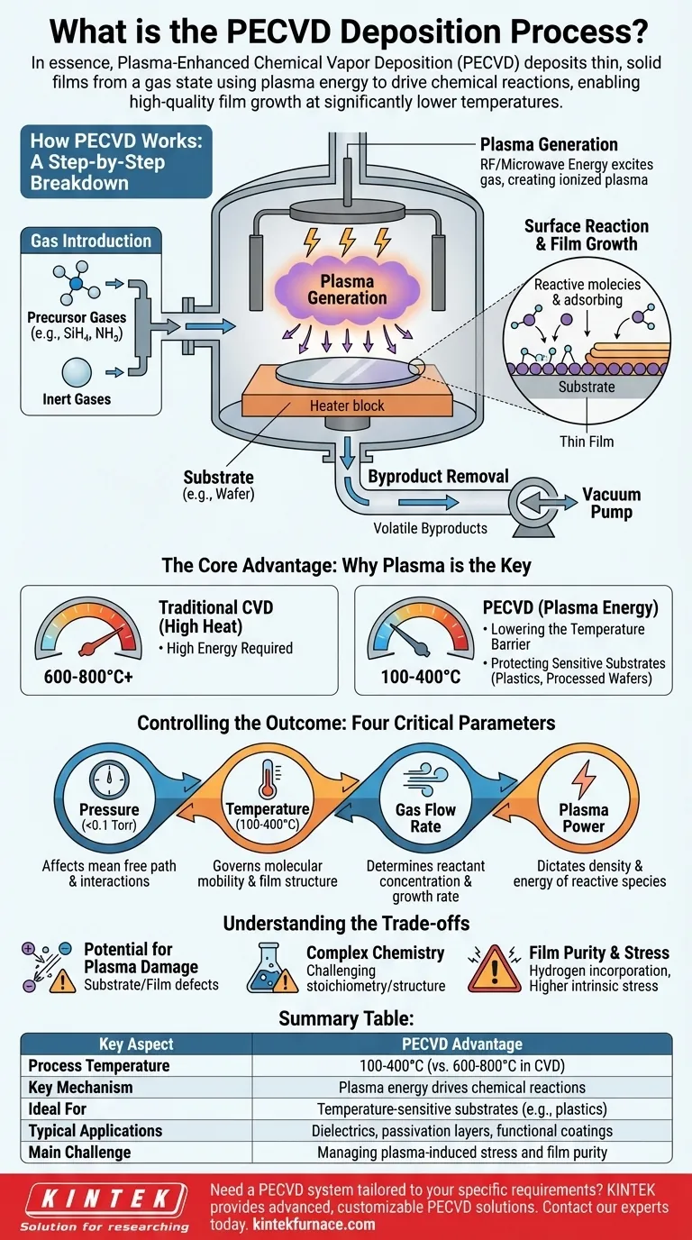
How PECVD Works: A Step-by-Step Breakdown
The PECVD process takes place inside a vacuum chamber and can be broken down into four primary stages.
Step 1: Gas Introduction
The process begins by introducing carefully controlled streams of precursor gases into the vacuum chamber. These gases, such as silane (SiH₄) and ammonia (NH₃), contain the elements needed to form the desired film. Inert gases are often mixed in to help manage the process.
Step 2: Plasma Generation
A powerful electric field, typically using radio frequency (RF) or microwave energy, is applied between two electrodes within the chamber. This energy excites the gas mixture, stripping electrons from atoms and creating a plasma—an ionized gas containing a mix of ions, electrons, and highly reactive neutral species. This is often visible as a characteristic glow discharge.
Step 3: Surface Reaction and Film Growth
The reactive chemical species generated in the plasma diffuse toward the substrate, which is heated to a controlled, moderate temperature. These activated molecules adsorb onto the substrate surface, undergo chemical reactions, and bond to the surface, building up the thin film layer by layer.
Step 4: Byproduct Removal
The chemical reactions on the surface create volatile byproducts. These waste gases are continuously removed from the chamber by the vacuum system, ensuring a clean deposition process and high-purity film.
The Core Advantage: Why Plasma is the Key
The use of plasma is what distinguishes PECVD and provides its main benefits. The energy required to break down the precursor gas molecules is supplied by the plasma, not just by thermal energy.
Lowering the Temperature Barrier
In traditional Chemical Vapor Deposition (CVD), temperatures of 600-800°C or higher are often necessary to provide enough energy for reactions to occur. In PECVD, the plasma provides this activation energy, allowing deposition to happen at much lower temperatures, often in the 100-400°C range.
Protecting Sensitive Substrates
This lower operating temperature is critical. It enables the deposition of films on materials that cannot withstand high heat, such as plastics, polymers, and semiconductor wafers that have already undergone previous processing steps.
Controlling the Outcome: The Four Critical Parameters
The final properties of the deposited film—such as its thickness, density, and stress—are determined by carefully controlling four key process variables.
Pressure
The pressure inside the chamber (typically <0.1 Torr) affects the "mean free path" of gas molecules, influencing how they interact before reaching the substrate.
Temperature
While lower than in CVD, the substrate temperature still plays a crucial role. It governs the mobility of molecules on the surface, which affects the film's final structure and density.
Gas Flow Rate
The rate at which precursor gases are supplied determines the concentration of reactants available for the deposition, directly influencing the film's growth rate and chemical composition.
Plasma Power
The amount of power applied to generate the plasma dictates the density and energy of the reactive species. This is a powerful lever for adjusting the film's growth rate and physical properties.
Understanding the Trade-offs
While powerful, PECVD is not without its complexities. The introduction of plasma adds variables that require careful management.
Potential for Plasma Damage
The high-energy ions within the plasma can bombard the substrate surface. While this can sometimes be beneficial (improving film density), uncontrolled bombardment can create defects or damage in the substrate or the growing film.
Complex Chemistry
The plasma environment creates a wide variety of reactive species, making the underlying chemistry more complex than in purely thermal processes. This can sometimes make it more challenging to achieve a specific film stoichiometry or crystalline structure.
Film Purity and Stress
Byproducts from the plasma reactions, particularly hydrogen, can become incorporated into the film, affecting its properties. Additionally, the lower deposition temperature can lead to higher intrinsic stress within the film compared to high-temperature methods.
Making the Right Choice for Your Goal
Selecting a deposition method depends entirely on your material constraints and desired film properties.
- If your primary focus is depositing on heat-sensitive materials: PECVD is an ideal, and often the only, choice due to its low-temperature nature.
- If your primary focus is the highest possible film purity and crystallinity: You may need to evaluate whether a higher-temperature process like Low-Pressure CVD (LPCVD) is more suitable, provided your substrate can tolerate the heat.
- If your primary focus is a fast, versatile, and cost-effective coating: PECVD offers excellent deposition rates and is widely used for creating functional films like dielectrics and passivation layers in industrial manufacturing.
By leveraging plasma to overcome thermal barriers, PECVD provides a versatile and indispensable tool for modern materials engineering.
Summary Table:
| Key Aspect | PECVD Advantage |
|---|---|
| Process Temperature | 100-400°C (vs. 600-800°C in CVD) |
| Key Mechanism | Plasma energy drives chemical reactions |
| Ideal For | Temperature-sensitive substrates (e.g., plastics, processed wafers) |
| Typical Applications | Dielectrics, passivation layers, functional coatings |
| Main Challenge | Managing plasma-induced stress and film purity |
Need a PECVD system tailored to your specific research or production requirements? KINTEK leverages exceptional R&D and in-house manufacturing to provide advanced PECVD solutions for diverse laboratories. Our deep customization capabilities ensure your system precisely meets unique experimental needs, whether you're working with sensitive substrates or require specific film properties. Contact our experts today to discuss how our PECVD and broader furnace portfolio can enhance your thin film processes.
Visual Guide
Related Products
- RF PECVD System Radio Frequency Plasma Enhanced Chemical Vapor Deposition
- Inclined Rotary Plasma Enhanced Chemical Deposition PECVD Tube Furnace Machine
- Slide PECVD Tube Furnace with Liquid Gasifier PECVD Machine
- Inclined Rotary Plasma Enhanced Chemical Deposition PECVD Tube Furnace Machine
- 915MHz MPCVD Diamond Machine Microwave Plasma Chemical Vapor Deposition System Reactor
People Also Ask
- What is RF in PECVD? A Critical Control for Plasma Deposition
- What are the key advantages of PECVD technology? Achieve Low-Temperature, High-Quality Thin Film Deposition
- How are deposition rates and film properties controlled in PECVD? Master Key Parameters for Optimal Thin Films
- How does film quality compare between PECVD and CVD? Choose the Best Method for Your Substrate
- What is the role of RF power in PECVD and how does the RF-PECVD process work? Master Thin Film Deposition Control


