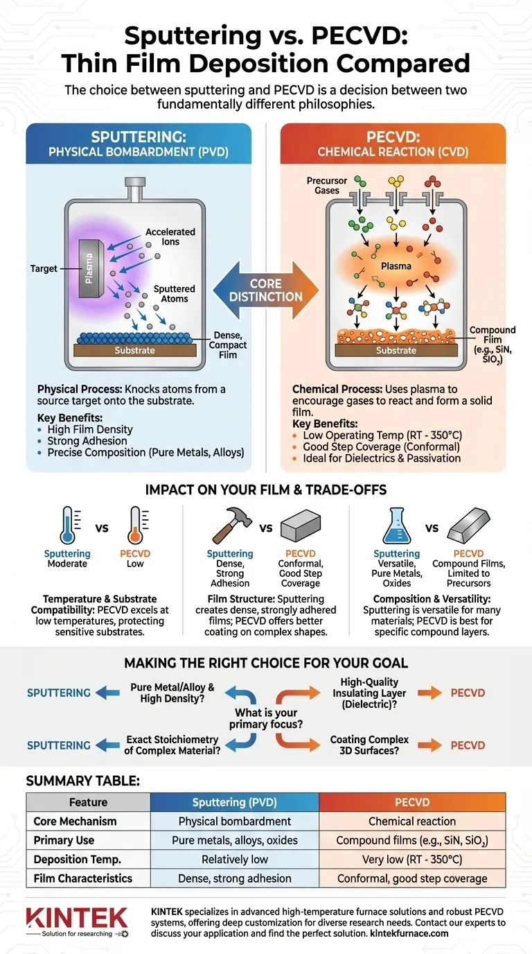
At its core, the difference between sputtering and Plasma-Enhanced Chemical Vapor Deposition (PECVD) lies in how they build a thin film. Sputtering is a physical process that knocks atoms from a source target onto your substrate, much like a microscopic sandblaster. In contrast, PECVD is a chemical process that uses plasma to encourage gases to react and form a solid film on the substrate's surface.
The choice between sputtering and PECVD is a decision between two fundamentally different philosophies. Sputtering offers precision and density by physically transferring material, while PECVD enables the creation of unique compound films at low temperatures through controlled chemical reactions.
The Core Distinction: Physical vs. Chemical Deposition
To select the right method, you must first understand their opposing mechanisms. One physically moves atoms, while the other chemically constructs molecules.
Sputtering: A Physical Bombardment Process
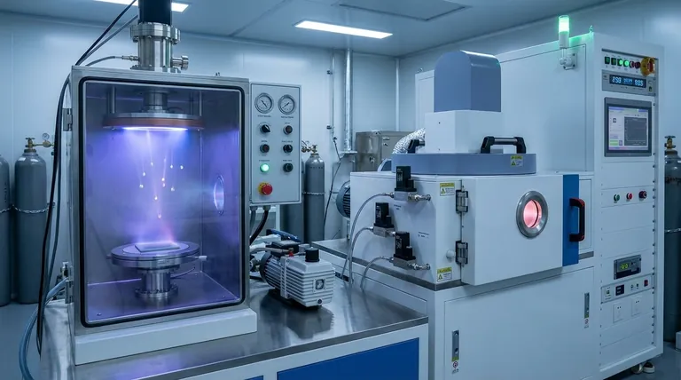
Sputtering is a type of Physical Vapor Deposition (PVD). The process begins by creating a plasma, typically from an inert gas like Argon.
These energized gas ions are accelerated and aimed at a block of source material, known as the target.
When the ions strike the target, they physically dislodge or "sputter" atoms from it. These ejected atoms then travel through the vacuum chamber and deposit onto the substrate, building the thin film layer by layer.
PECVD: A Plasma-Assisted Chemical Reaction
PECVD is a variant of Chemical Vapor Deposition (CVD). Instead of a solid target, this process uses reactive precursor gases.
A plasma is used to transfer energy into these gases, breaking their chemical bonds and creating highly reactive molecules.
These reactive species then settle on the substrate, where they undergo a chemical reaction to form the desired solid thin film. The plasma allows this reaction to occur at much lower temperatures than in traditional CVD.
How This Difference Impacts Your Film
The mechanism—physical transfer versus chemical reaction—directly influences the temperature, structure, and composition of the resulting film.
Deposition Temperature and Substrate Compatibility
PECVD's primary advantage is its low operating temperature, often between room temperature and 350°C. The plasma provides the energy for chemical reactions that would otherwise require extreme heat (600°C+).
This makes PECVD ideal for depositing films on temperature-sensitive substrates like plastics or semiconductor wafers that already contain delicate integrated circuits.
While sputtering is also a relatively low-temperature process, the key benefit of PECVD is enabling chemical deposition without the damaging heat of conventional CVD.
Film Density and Adhesion
Sputtered atoms arrive at the substrate with significant kinetic energy. This "hammering" effect typically results in very dense, compact films with strong adhesion to the substrate.
This is highly desirable for applications like electrical contacts, diffusion barriers, or reflective coatings where film integrity is paramount.
Film Composition and Structure
Sputtering excels at depositing films of pure metals, alloys, and oxides with high fidelity. The composition of the film is a direct reflection of the target material, offering precise control.
PECVD, by nature, is used to synthesize compound films, particularly amorphous ones like silicon nitride (SiN) or silicon dioxide (SiO₂). It is less suited for depositing pure metals but is the industry standard for creating high-quality dielectric and passivation layers.
Understanding the Trade-offs
Neither method is universally superior. The optimal choice depends entirely on your specific material and performance requirements.
Material Versatility
Sputtering is more versatile for a wider range of materials. As long as you can form a material into a solid target, you can likely sputter it.
PECVD is limited by the availability of suitable precursor gases that are stable at room temperature but will react appropriately within the plasma.
Deposition Rate vs. Step Coverage
PECVD can often achieve higher deposition rates, which is beneficial for manufacturing thicker films.
However, sputtering generally provides better thickness uniformity across large substrates. PECVD films also tend to be more conformal, meaning they can coat the sides of complex, three-dimensional surface features more evenly than the more directional, "line-of-sight" sputtering process.
Making the Right Choice for Your Goal
Base your decision on the properties you need in your final film, not on the process itself.
- If your primary focus is depositing a pure metal or alloy with high density: Sputtering is the superior choice due to its physical transfer mechanism and precise control.
- If your primary focus is creating a high-quality insulating layer (dielectric) on a temperature-sensitive substrate: PECVD is the ideal solution, as it was specifically designed for this purpose.
- If your primary focus is maintaining the exact stoichiometry of a complex compound material: Sputtering from a pre-made target provides the most direct and controllable path.
- If your primary focus is coating a complex surface with a uniform, conformal layer: PECVD's gas-phase reaction mechanism often provides better step coverage.
Ultimately, understanding the fundamental difference between physical bombardment and chemical reaction will empower you to select the correct tool for your specific engineering challenge.
Summary Table:
| Feature | Sputtering (PVD) | PECVD |
|---|---|---|
| Core Mechanism | Physical bombardment | Chemical reaction |
| Primary Use | Pure metals, alloys, oxides | Compound films (e.g., SiN, SiO₂) |
| Deposition Temp. | Relatively low | Very low (RT - 350°C) |
| Film Characteristics | Dense, strong adhesion | Conformal, good step coverage |
Still unsure which deposition method is right for your project?
KINTEK specializes in advanced high-temperature furnace solutions, including our robust PECVD systems. Leveraging exceptional R&D and in-house manufacturing, we provide diverse laboratories with the right tools for their unique challenges. Our strong deep customization capability ensures we can precisely meet your specific experimental requirements.
Contact our experts today to discuss your application and find the perfect solution for your thin film deposition needs.
Visual Guide
Related Products
- Spark Plasma Sintering SPS Furnace
- High Temperature Muffle Oven Furnace for Laboratory Debinding and Pre Sintering
People Also Ask
- What are the key differences between SiC and MoSi2 heating elements in sintering furnaces? Choose the Right Element for Your High-Temp Needs
- What are the steps in the discharge plasma sintering process? Master Fast, High-Density Material Consolidation
- Why is it necessary to maintain a high vacuum environment during the SPS of SiC? Key to High-Density Ceramics
- What are the advantages of spark plasma sintering (SPS) over traditional forging? Precision Microstructural Control
- What is the significance of high-precision temperature monitoring systems in SPS? Control Ti-6Al-4V/HA Microstructure

