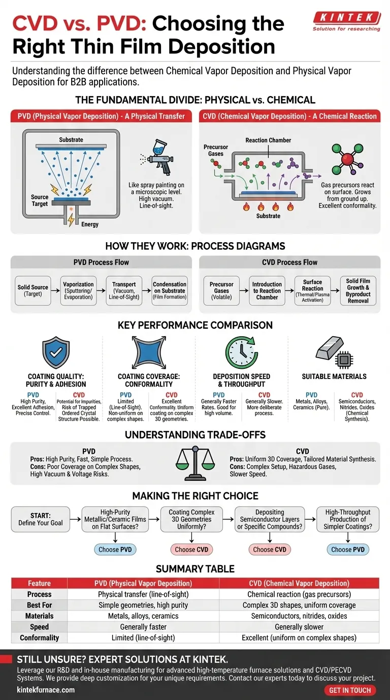
At its core, the difference between Chemical Vapor Deposition (CVD) and Physical Vapor Deposition (PVD) lies in how the coating material travels to and forms on a surface. PVD is a physical process that transfers a solid material into a vapor phase and deposits it, much like spray painting on a microscopic level. In contrast, CVD is a chemical process where gas precursors react on the substrate's surface to grow a new material layer from the ground up.
The choice between PVD and CVD is not about which is universally "better," but which is the right tool for a specific engineering goal. PVD excels at depositing pure, dense films with precise control on simple geometries, while CVD's strength is its unmatched ability to uniformly coat complex, three-dimensional surfaces.
The Fundamental Divide: Physical vs. Chemical Deposition
Understanding the core mechanism of each technique is the key to selecting the correct one for your application. They represent two fundamentally different philosophies for building a thin film.
How PVD Works: A Physical Transfer
Physical Vapor Deposition operates in a high-vacuum environment. A solid source material (a "target") is bombarded with energy, causing it to vaporize.
This vapor then travels in a straight line-of-sight path and condenses onto the cooler substrate, forming a thin film. The composition of the film is essentially identical to the source material.
How CVD Works: A Chemical Reaction
Chemical Vapor Deposition introduces one or more volatile gaseous precursors into a reaction chamber. These gases are not the final coating material itself.
When these gases encounter the heated substrate, a chemical reaction is triggered on its surface. This reaction forms the desired solid film material, and volatile byproducts are pumped away.
Comparing Key Performance Characteristics
The difference in mechanism leads to significant differences in performance, cost, and application suitability.
Coating Quality: Purity and Adhesion
PVD is renowned for producing films of exceptionally high purity and density, provided the source material is pure. The physical transfer process introduces very few contaminants.
This often results in films with excellent adhesion and precisely controlled properties, making PVD ideal for applications like optical coatings or wear-resistant tool coatings.
Coating Coverage: Conformality on Complex Shapes
This is CVD's signature advantage. Because the deposition is driven by a chemical reaction from a pervasive gas, it can occur on every exposed surface of a component simultaneously.
CVD offers superior conformality, meaning it can create a perfectly uniform coating layer inside deep trenches, around sharp corners, and on highly complex 3D geometries. PVD's line-of-sight nature makes this nearly impossible.
Deposition Speed and Throughput
Generally, PVD processes have faster deposition rates than CVD. This makes PVD a more economical choice for applications requiring thick films or high-volume production on relatively simple parts.
CVD's reliance on chemical reaction kinetics often makes it a slower, more deliberate process.
Suitable Materials
PVD is extremely versatile for depositing pure metals, alloys, and many ceramics.
CVD is the go-to method for materials that are best formed via chemical reaction, such as semiconductors (e.g., silicon), and specific compounds like nitrides and oxides that require precise chemical synthesis during deposition.
Understanding the Trade-offs
Neither method is a perfect solution. The choice involves balancing process complexity against performance requirements.
Process Complexity and Safety
PVD systems are mechanically complex but conceptually simpler. The primary hazards are related to high voltage and vacuum systems.
CVD is often more chemically complex, involving the handling of volatile, and sometimes toxic or corrosive, precursor gases. This adds significant safety and facility requirements.
Impurities and Defects
While PVD is inherently clean, CVD processes carry a risk of introducing impurities from unreacted precursor gases or chemical byproducts becoming trapped in the film.
However, the chemical growth of a CVD film can sometimes result in a more ordered crystalline structure than a condensed PVD film, which can be an advantage for certain electronic or optical applications.
Making the Right Choice for Your Goal
To select the correct method, you must first define your most critical outcome.
- If your primary focus is high-purity metallic or ceramic films on flat surfaces: Choose PVD for its speed, purity, and precise control over film properties.
- If your primary focus is coating complex 3D geometries uniformly: Choose CVD for its unparalleled conformality, ensuring complete and even coverage.
- If your primary focus is depositing semiconductor layers or specific chemical compounds (e.g., silicon nitride): Choose CVD, as the process is fundamentally designed for this type of chemical synthesis.
- If your primary focus is high-throughput production of simpler wear or decorative coatings: Choose PVD due to its generally faster deposition rates.
Ultimately, selecting the right deposition technology begins with a clear understanding of your material requirements and the geometry of the part you need to coat.
Summary Table:
| Feature | PVD (Physical Vapor Deposition) | CVD (Chemical Vapor Deposition) |
|---|---|---|
| Process | Physical transfer (line-of-sight) | Chemical reaction (gas precursors) |
| Best For | Simple geometries, high purity | Complex 3D shapes, uniform coverage |
| Materials | Metals, alloys, ceramics | Semiconductors, nitrides, oxides |
| Speed | Generally faster | Generally slower |
| Conformality | Limited (line-of-sight) | Excellent (uniform on complex shapes) |
Still unsure whether PVD or CVD is right for your specific application?
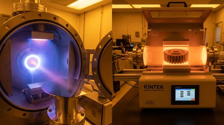
At KINTEK, we leverage our exceptional R&D and in-house manufacturing capabilities to provide advanced high-temperature furnace solutions, including specialized CVD/PECVD Systems. Our expertise in thin film deposition technologies allows us to offer deep customization to precisely meet your unique experimental and production requirements.
Contact our experts today to discuss your project's specific needs and discover how our tailored solutions can enhance your coating process. Get in touch via our contact form for a personalized consultation.
Visual Guide
Related Products
- Custom Made Versatile CVD Tube Furnace Chemical Vapor Deposition CVD Equipment Machine
- HFCVD Machine System Equipment for Drawing Die Nano Diamond Coating
- 915MHz MPCVD Diamond Machine Microwave Plasma Chemical Vapor Deposition System Reactor
- RF PECVD System Radio Frequency Plasma Enhanced Chemical Vapor Deposition
- Multi Heating Zones CVD Tube Furnace Machine for Chemical Vapor Deposition Equipment
People Also Ask
- What customization options are available for CVD tube furnaces? Tailor Your System for Superior Material Synthesis
- What future trends are expected in the development of CVD tube furnaces? Discover Smarter, More Versatile Systems
- Which industries and research fields benefit from CVD tube furnace sintering systems for 2D materials? Unlock Next-Gen Tech Innovations
- How might AI and machine learning enhance CVD tube furnace processes? Boost Quality, Speed, and Safety
- Why are CVD tube furnace sintering systems indispensable for 2D material research and production? Unlock Atomic-Scale Precision


