At its core, Plasma-Enhanced Chemical Vapor Deposition (PECVD) is a sophisticated manufacturing process used to deposit exceptionally thin films of material onto a substrate. Unlike traditional methods that rely on extreme heat, PECVD uses an energized gas, or plasma, to drive the chemical reactions needed to build the film layer by layer. This allows the process to run at significantly lower temperatures, making it indispensable for modern electronics and materials science.
The central challenge in thin-film deposition has always been applying high-quality coatings without damaging the underlying material with heat. PECVD solves this by using plasma as a substitute for thermal energy, enabling the creation of advanced films on temperature-sensitive substrates that would otherwise be impossible to process.
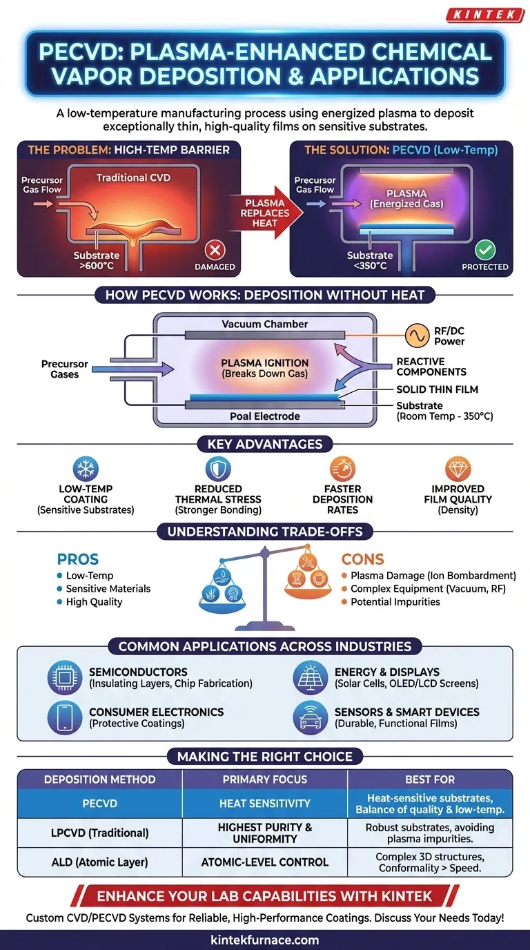
The Core Problem: The Temperature Barrier in Deposition
Traditional thin-film coating relies on a process called Chemical Vapor Deposition (CVD). This method works by heating a substrate to very high temperatures, often over 600°C, inside a chamber filled with precursor gases.
The Limitation of High Heat
The intense heat provides the activation energy required for the gas molecules to react and deposit a solid film onto the substrate's surface. While effective, this high-temperature requirement creates a significant limitation.
Many advanced materials, such as polymers, certain semiconductor devices, or previously fabricated integrated circuits, cannot withstand such heat. Exposing them to traditional CVD temperatures would cause them to melt, warp, or degrade, destroying the component.
How PECVD Solves the Problem: Deposition Without the Heat
PECVD, sometimes called Plasma-Assisted CVD (PACVD), was developed specifically to overcome this temperature barrier. It fundamentally changes how the activation energy is supplied to the chemical reaction.
The Role of Plasma
Instead of relying solely on thermal energy, PECVD introduces energy by creating a plasma within the reaction chamber. This plasma is a highly energized state of gas, generated by applying an electric field (typically radio frequency or DC).
The energetic plasma collides with the precursor gas molecules, breaking them down into reactive components. This "pre-digestion" of the gases provides the necessary energy for the deposition reaction to occur without needing to heat the entire chamber to extreme temperatures.
The Deposition Process Explained
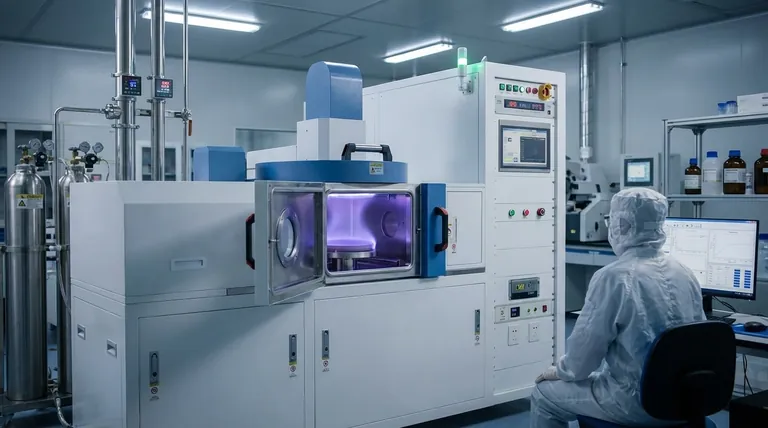
The process occurs at much lower substrate temperatures, typically between room temperature and 350°C. Reactant gases are introduced between parallel electrodes inside a vacuum chamber.
The electric field ignites the plasma, which decomposes the gases. These reactive chemical species then land on the cooler substrate and form a solid, high-quality thin film. By precisely controlling the gas mixture and plasma conditions, engineers can tune the exact properties of the deposited layer.
Key Advantages of the PECVD Method
This plasma-driven approach results in several key benefits. It allows for the coating of temperature-sensitive substrates, reduces thermal stress on the film, and can lead to stronger bonding at interfaces.
Furthermore, PECVD often enables faster deposition rates and produces films with improved density and quality compared to other low-temperature techniques.
Understanding the Trade-offs
While powerful, PECVD is not a universal solution. The use of an energetic plasma introduces its own set of considerations that make it different from purely thermal processes.
Potential for Plasma Damage
The same high-energy ions that enable low-temperature deposition can sometimes cause physical damage (ion bombardment) to extremely sensitive substrate surfaces or the film itself. This requires careful process tuning to mitigate.
Process and Equipment Complexity
PECVD systems are inherently more complex than their thermal CVD counterparts. The need for vacuum chambers, gas delivery systems, and radio-frequency (RF) power generators makes the equipment more expensive to purchase and maintain.
Film Chemistry Complications
The plasma environment is a complex chemical soup. This can sometimes lead to the unintentional incorporation of other elements, like hydrogen, into the film, which may alter its desired electrical or optical properties.
Common Applications Across Industries
The ability to deposit high-quality films at low temperatures has made PECVD a cornerstone technology in numerous high-tech fields.
Semiconductor and Electronics Manufacturing
PECVD is essential for fabricating modern integrated circuits. It's used to deposit insulating layers (like silicon dioxide and silicon nitride) between metal layers on a chip, a process that must be done at low temperatures to avoid damaging the underlying transistors.
It is also critical in consumer electronics like smartphones, wearables, and hearables for creating protective and functional coatings.
Energy and Display Technologies
The technology is widely used in the production of photovoltaics (solar cells) and advanced display technologies like LCD and OLED screens. It enables the efficient deposition of anti-reflective coatings and electronically active layers that are crucial for device performance.
Sensors and Smart Devices
From automotive sensors to biosensors and smart utility meters, PECVD provides the durable, high-performance coatings needed for reliable operation. These films protect sensitive components from the environment while providing essential insulating or conductive properties.
Making the Right Choice for Your Goal
Selecting a deposition method depends entirely on the material constraints and desired outcome of your project.
- If your primary focus is coating heat-sensitive substrates: PECVD is the industry-standard choice, offering an unmatched balance of quality and low-temperature compatibility.
- If your primary focus is achieving the highest possible film purity and uniformity on a robust substrate: A traditional high-temperature process like Low-Pressure CVD (LPCVD) may be superior, as it avoids potential plasma-induced impurities.
- If your primary focus is atomic-level thickness control on complex 3D structures: You may need to consider an alternative like Atomic Layer Deposition (ALD), which offers superior conformality at the expense of speed.
By understanding its unique ability to decouple the deposition reaction from high heat, you can effectively leverage PECVD to build the next generation of advanced materials and devices.
Summary Table:
| Aspect | Details |
|---|---|
| Process | Uses plasma to deposit thin films at low temperatures (room temp to 350°C) |
| Key Advantages | Enables coating of temperature-sensitive substrates, faster deposition, high film quality |
| Common Applications | Semiconductor manufacturing, solar cells, display technologies, sensors |
| Limitations | Potential plasma damage, higher equipment complexity, possible film impurities |
Ready to enhance your lab's capabilities with advanced PECVD solutions? KINTEK leverages exceptional R&D and in-house manufacturing to provide high-temperature furnace solutions, including CVD/PECVD Systems, tailored for diverse laboratories. Our strong deep customization capability ensures we precisely meet your unique experimental requirements, delivering reliable, high-performance coatings for semiconductors, energy devices, and more. Contact us today to discuss how we can support your innovation and efficiency goals!
Visual Guide
Related Products
- RF PECVD System Radio Frequency Plasma Enhanced Chemical Vapor Deposition
- Slide PECVD Tube Furnace with Liquid Gasifier PECVD Machine
- Inclined Rotary Plasma Enhanced Chemical Deposition PECVD Tube Furnace Machine
- Inclined Rotary Plasma Enhanced Chemical Deposition PECVD Tube Furnace Machine
- Cylindrical Resonator MPCVD Machine System for Lab Diamond Growth
People Also Ask
- What are some promising applications of PECVD-prepared 2D materials? Unlock Advanced Sensing and Optoelectronics
- How are deposition rates and film properties controlled in PECVD? Master Key Parameters for Optimal Thin Films
- What is RF in PECVD? A Critical Control for Plasma Deposition
- What is PECVD specification? A Guide to Choosing the Right System for Your Lab
- What are the applications of plasma enhanced chemical vapor deposition? Key Uses in Electronics, Optics & Materials


