In the semiconductor industry, Plasma-Enhanced Chemical Vapor Deposition (PECVD) is a process used to deposit very thin, uniform films of material onto a silicon wafer at relatively low temperatures. Unlike traditional Chemical Vapor Deposition (CVD) which requires high heat, PECVD uses an energized gas, or plasma, to drive the chemical reactions needed to create the film. This low-temperature capability is essential for modern chip manufacturing.
The central role of PECVD is to enable the construction of complex, multi-layered microchips. It allows for the deposition of critical insulating and protective films without using high temperatures that would otherwise damage the delicate transistor structures already built on the wafer.
The Core Problem PECVD Solves: Heat
To understand PECVD's importance, you must first understand the primary limitation of its predecessor, traditional Chemical Vapor Deposition (CVD).
The Limits of High-Temperature Deposition
Traditional CVD processes rely on high temperatures, often exceeding 600-800°C, to provide the energy needed for precursor gases to react and form a solid film on the wafer.
While effective, this extreme heat is destructive to the intricate, multi-layered circuitry of a modern semiconductor device.
Why Low Temperature is Non-Negotiable
As a chip is fabricated, layers of microscopic transistors and wiring are built up. These pre-existing structures are highly sensitive.
Exposing them to the high temperatures of traditional CVD would cause dopants to diffuse out of place, materials to degrade, and ultimately, the entire integrated circuit to fail. Modern chipmaking is often a "low thermal budget" process.
How Plasma Replaces Heat
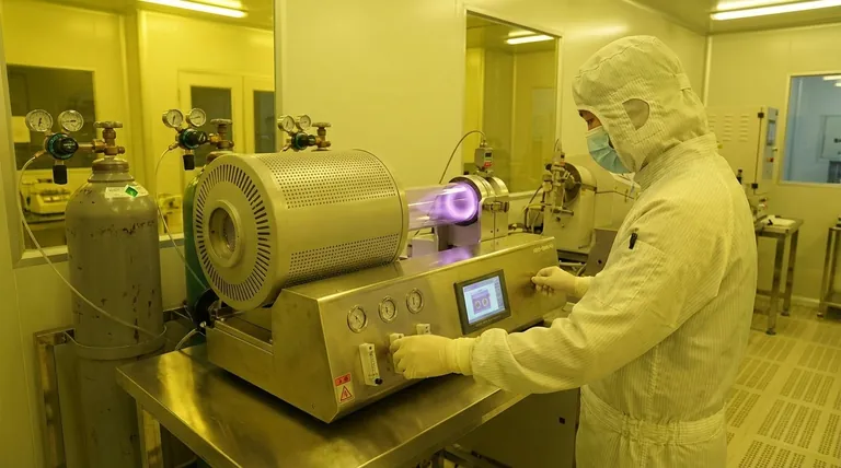
PECVD circumvents this problem by introducing energy in a different form: a plasma.
By applying an electromagnetic field (typically radio frequency), precursor gases are ionized into a highly reactive state. This plasma provides the necessary energy to drive the chemical reaction, allowing a high-quality film to form on the wafer at much lower temperatures, typically 200-400°C.
Key PECVD Applications in Chip Fabrication
PECVD is not a niche process; it is a workhorse used to create several types of essential layers on nearly every modern chip.
Dielectric Layers for Isolation
PECVD is a primary method for depositing silicon dioxide (SiO₂). These films act as insulators, electrically isolating the vast network of metal interconnects (wires) that connect the millions or billions of transistors on a chip, preventing short circuits.
Passivation Layers for Protection
One of the most common applications is depositing a final silicon nitride (Si₃N₄) layer. This tough, dense film acts as a protective shell, or passivation layer, sealing the completed chip from moisture, mobile ions, and other contaminants that could cause it to fail over time.
Advanced Films for Performance
In advanced microprocessors, speed is limited by the delay in signals traveling through the copper wiring. PECVD is used to deposit low-k dielectric films, which are specialized insulators that reduce this delay, allowing the chip to operate at higher frequencies.
Understanding the Advantages and Trade-offs
No single process is perfect for every application. PECVD is chosen for its unique balance of capabilities.
The Primary Advantage: Process Control
Beyond low temperature, PECVD systems offer exceptional control over the properties of the deposited film. Engineers can finely tune film thickness, uniformity, and mechanical stress. Controlling stress is vital to prevent the deposited film from cracking or warping the wafer.
Versatility Across Materials
The process is highly versatile, capable of depositing a wide range of materials, including silicon dioxide, silicon nitride, amorphous silicon, and more complex compounds used in specialized devices like thin-film transistors (TFTs) for displays.
The Inherent Trade-off: Film Purity
The primary trade-off for operating at low temperatures is that PECVD films can contain more impurities, such as hydrogen, than films grown with high-temperature methods. For many applications like passivation, this is perfectly acceptable. However, for the most sensitive layers, like the gate dielectric directly on a transistor, a higher-temperature, higher-purity process is often required if the thermal budget allows.
Applying This to Fabrication Goals
An engineer's choice of deposition method is always driven by the specific requirements of the layer being built.
- If your primary focus is depositing an insulator after transistors are built: PECVD is the definitive choice because its low temperature protects the underlying sensitive structures.
- If your primary focus is creating an ultra-pure, dense foundational layer: A higher-temperature process like Low-Pressure CVD (LPCVD) might be chosen, but only if it's applied early in manufacturing before temperature-sensitive components exist.
- If your primary focus is sealing a finished chip from the environment: PECVD is the industry standard for depositing the final silicon nitride passivation layer due to its excellent protective qualities and process safety.
Ultimately, PECVD is a cornerstone technology that makes the vertical complexity of modern integrated circuits possible.
Summary Table:
| Key Aspect | PECVD's Role |
|---|---|
| Core Advantage | Enables film deposition at low temperatures (200-400°C) to protect delicate chip structures. |
| Primary Applications | Deposition of silicon dioxide (SiO₂) insulators, silicon nitride (Si₃N₄) passivation layers, and advanced low-k dielectric films. |
| Key Limitation | Films may contain more impurities (e.g., hydrogen) compared to high-temperature deposition methods. |
| Ideal Use Case | Essential for adding layers after temperature-sensitive transistors and wiring are built on the wafer. |
Ready to Integrate Advanced PECVD Technology into Your Lab?
Leveraging exceptional R&D and in-house manufacturing, KINTEK provides semiconductor and advanced materials laboratories with precisely engineered PECVD solutions. Our systems are designed to deliver the exceptional process control, uniformity, and low-temperature performance required for cutting-edge research and development.
Our product line, including PECVD/CVD Systems, Tube Furnaces, and Vacuum & Atmosphere Furnaces, is complemented by our strong deep customization capability to precisely meet your unique experimental and process requirements.
Contact our experts today to discuss how our PECVD solutions can accelerate your semiconductor fabrication or thin-film research.
Visual Guide

Related Products
- Slide PECVD Tube Furnace with Liquid Gasifier PECVD Machine
- RF PECVD System Radio Frequency Plasma Enhanced Chemical Vapor Deposition
- Inclined Rotary Plasma Enhanced Chemical Deposition PECVD Tube Furnace Machine
- Inclined Rotary Plasma Enhanced Chemical Deposition PECVD Tube Furnace Machine
- Multi Heating Zones CVD Tube Furnace Machine for Chemical Vapor Deposition Equipment
People Also Ask
- What plasma source is used in PE-CVD tube furnaces? Unlock Low-Temperature, High-Quality Deposition
- What are the main advantages of PECVD tube furnaces compared to CVD tube furnaces? Lower Temp, Faster Deposition, and More
- What are the typical conditions for plasma-enhanced CVD processes? Achieve Low-Temperature Thin Film Deposition
- What is plasma in the context of PECVD? Unlock Low-Temperature Thin Film Deposition
- What role does a Tube Furnace play in the CVD growth of carbon nanotubes? Achieve High-Purity CNT Synthesis


