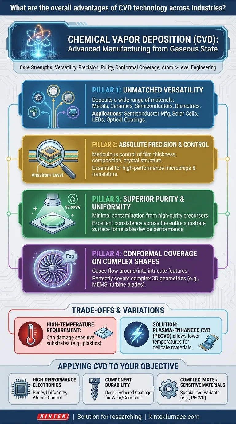
At its core, Chemical Vapor Deposition (CVD) is an advanced manufacturing process that builds high-performance, ultra-thin films of material from a gaseous state. Its primary advantages are its exceptional versatility to deposit a wide range of materials, its precision in controlling film thickness and composition, and its ability to create coatings of superior purity, uniformity, and adhesion, even on complex surfaces.
The true power of CVD is not just in applying a coating, but in enabling atomic-level engineering. It allows innovators to build materials from the ground up, designing specific properties like hardness, conductivity, or optical transparency directly into a component.
The Pillars of CVD's Widespread Adoption
The advantages of CVD are not isolated benefits; they work together to solve critical challenges in modern manufacturing, from microelectronics to heavy industry. Understanding these pillars clarifies why it has become a foundational technology.
Pillar 1: Unmatched Versatility
CVD is not a single process but a family of techniques capable of depositing an enormous variety of materials. This includes metals, ceramics, semiconductors, and dielectrics.
This flexibility makes it invaluable across disparate fields. It is used for creating silicon-based films in semiconductor manufacturing, transparent conductive oxides for solar cells, and specialized optical coatings for LEDs and laser diodes.
Pillar 2: Absolute Precision and Control
The process allows for meticulous control over the final product. By precisely adjusting precursor gases, temperature, and pressure, engineers can dictate the film's exact thickness, chemical composition, and crystal structure.
This level of control is non-negotiable for high-performance applications. In microchips, for example, layers must be deposited with angstrom-level precision to create functional transistors. CVD provides this repeatability and fine-tuning.
Pillar 3: Superior Purity and Uniformity
CVD reactions use highly pure precursor gases, resulting in deposited films with minimal contamination. This purity is critical for the performance of electronic and optical devices, where even trace impurities can cause catastrophic failure.
Furthermore, the process ensures the film is applied with excellent uniformity across the entire substrate surface. This consistency is vital for ensuring that every chip on a silicon wafer or every part in a batch performs identically.
Pillar 4: Conformal Coverage on Complex Shapes
Unlike line-of-sight deposition techniques (like sputtering), CVD gases can flow around and into intricate features. This results in a "conformal" coating that perfectly covers complex, three-dimensional geometries with a uniform thickness.
Imagine trying to paint a complex chain-link fence with a spray can; you would miss many spots. CVD acts more like a fog that settles evenly on every single surface, making it ideal for coating complex parts like turbine blades or the internal structures of micro-electromechanical systems (MEMS).
Understanding the Trade-offs and Variations
While powerful, CVD is not a universal solution. Understanding its limitations is key to making an informed decision.
The High-Temperature Requirement
Traditional CVD processes often require very high temperatures (several hundred to over a thousand degrees Celsius) to drive the necessary chemical reactions.
This heat can damage or destroy thermally sensitive substrates, such as plastics or certain electronic components that have already been fabricated on a wafer.
The Rise of Low-Temperature CVD
To overcome this limitation, specialized variations have been developed. Plasma-Enhanced CVD (PECVD), for example, uses an energy-rich plasma to initiate the reaction.
This allows for deposition at much lower temperatures, protecting delicate substrates and opening up new applications in flexible electronics and advanced semiconductor manufacturing.
Precursor Handling and Cost
The gases used in CVD can be toxic, flammable, or corrosive, necessitating significant investment in safety protocols, exhaust treatment, and facility infrastructure. The high purity of these precursors can also contribute to the overall cost of the process.
Applying CVD to Your Objective
Choosing the right deposition technology depends entirely on your end goal.
- If your primary focus is high-performance electronics: The purity, uniformity, and atomic-level control of CVD are essential for manufacturing reliable microchips, sensors, and optoelectronics.
- If your primary focus is component durability: CVD provides exceptionally dense, pure, and well-adhered coatings for superior wear, corrosion, and thermal resistance on tools, engine parts, and aerospace components.
- If your primary focus is coating complex parts or sensitive materials: You must investigate specific CVD variants. Standard CVD is ideal for complex shapes that can withstand heat, while low-temperature processes like PECVD are required for polymers or pre-processed wafers.
CVD is less a single tool and more a master key, unlocking the ability to design and build the next generation of advanced materials.
Summary Table:
| Pillar | Key Advantage | Key Applications |
|---|---|---|
| Versatility | Deposits a wide range of materials (metals, ceramics, semiconductors) | Semiconductor manufacturing, solar cells, LEDs |
| Precision and Control | Meticulous control over film thickness and composition | Microchips, high-performance electronics |
| Purity and Uniformity | High-purity films with excellent consistency across substrates | Optical devices, batch manufacturing |
| Conformal Coverage | Uniform coating on complex 3D geometries | Turbine blades, MEMS, intricate parts |
Ready to elevate your material engineering with advanced CVD solutions? At KINTEK, we leverage exceptional R&D and in-house manufacturing to provide diverse laboratories with cutting-edge high-temperature furnace solutions. Our product line, including Muffle, Tube, Rotary Furnaces, Vacuum & Atmosphere Furnaces, and CVD/PECVD Systems, is complemented by strong deep customization capabilities to precisely meet your unique experimental requirements. Whether you're in semiconductors, aerospace, or other high-tech fields, we can help you achieve superior coatings and performance. Contact us today to discuss how our tailored solutions can benefit your projects!
Visual Guide
Related Products
- Custom Made Versatile CVD Tube Furnace Chemical Vapor Deposition CVD Equipment Machine
- Multi Heating Zones CVD Tube Furnace Machine for Chemical Vapor Deposition Equipment
- HFCVD Machine System Equipment for Drawing Die Nano Diamond Coating
- Split Chamber CVD Tube Furnace with Vacuum Station CVD Machine
- 915MHz MPCVD Diamond Machine Microwave Plasma Chemical Vapor Deposition System Reactor
People Also Ask
- What are the practical applications of gate media prepared by CVD tube furnaces? Unlock Advanced Electronics and More
- How does CVD tube furnace sintering enhance graphene growth? Achieve Superior Crystallinity and High Electron Mobility
- What are the benefits of developing new precursor materials for CVD tube furnaces? Unlock Advanced Thin-Film Synthesis
- What is the working principle of a CVD tube furnace? Achieve Precise Thin Film Deposition for Your Lab
- Why are CVD tube furnace sintering systems indispensable for 2D material research and production? Unlock Atomic-Scale Precision


