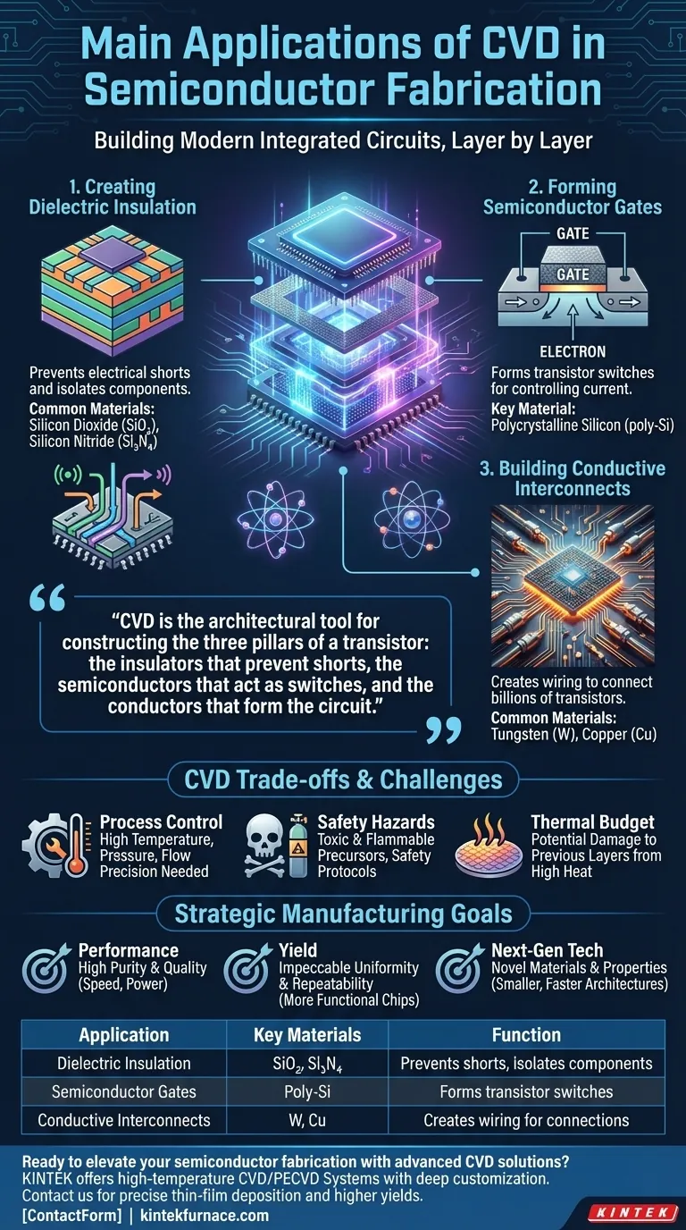
In semiconductor fabrication, Chemical Vapor Deposition (CVD) is the foundational process for building the complex, multi-layered structures that form modern integrated circuits. Its primary applications involve depositing thin films that serve one of three critical functions: providing electrical insulation, forming the active semiconductor components, or creating the conductive wiring that connects everything together.
Understanding CVD is not just about knowing the materials it deposits, but recognizing it as the architectural tool for constructing the three pillars of a transistor: the insulators that prevent shorts, the semiconductors that act as switches, and the conductors that form the circuit.
The Anatomy of a Chip: Where CVD Fits In
A modern microchip is not a flat object; it's a three-dimensional skyscraper with billions of components built layer by painstaking layer. CVD is the primary method used to construct many of these essential layers with atomic-level precision.
Application 1: Creating Dielectric Insulation
Every complex circuit needs insulation to prevent electrical current from leaking or short-circuiting between different components. CVD excels at depositing these non-conductive, or dielectric, layers.
These films isolate conductive pathways and electrically separate adjacent transistors from one another, ensuring signals go only where they are intended.
Common dielectric materials deposited via CVD include silicon dioxide (SiO₂) and silicon nitride (Si₃N₄).
Application 2: Forming Semiconductor Gates
The core of a transistor is the gate, which acts as a switch, controlling the flow of electricity. CVD is used to deposit the material for this critical component.
Polycrystalline silicon (poly-Si) is the most common material deposited by CVD for this purpose. The electrical properties and precise thickness of the poly-Si gate are fundamental to the transistor's performance and switching speed.
Application 3: Building Conductive Interconnects
With billions of transistors on a single chip, an incredibly dense network of "wiring" is needed to connect them. These pathways are known as interconnects.
CVD is used to deposit conductive films into tiny trenches etched into the chip's surface, forming this intricate wiring. Materials like tungsten (W) are commonly used to create contacts and plugs, while copper (Cu) is used for the main interconnect lines in more advanced chips.
Understanding the Trade-offs
While indispensable, CVD is a highly complex process with inherent challenges that engineers must manage to ensure successful manufacturing.
Process Control is Paramount
The quality of a CVD film depends on a delicate balance of temperature, pressure, and precursor gas flow rates. Even minor deviations can introduce defects, ruining entire batches of expensive silicon wafers.
Achieving a perfectly uniform film across a 300mm wafer is a significant engineering challenge. Non-uniformity leads to variations in device performance across the chip.
Material and Safety Hazards
The precursor gases used in CVD are often highly toxic, flammable, or corrosive. This necessitates extensive safety systems and specialized handling protocols, adding significant cost and complexity to the fabrication facility (fab).
Thermal Budget Constraints
Many CVD processes require very high temperatures. In a multi-step manufacturing sequence, applying this heat can potentially damage or alter layers that were deposited earlier in the process. Engineers must carefully manage the "thermal budget" of the entire fabrication flow.
Making the Right Choice for Your Goal
The specific application of CVD is always tied to a strategic manufacturing goal. Understanding this link is key to appreciating its role.
- If your primary focus is raw device performance: The purity and structural quality of CVD-deposited gate (poly-Si) and dielectric films are your most critical variables, as defects directly impact transistor speed and power consumption.
- If your primary focus is manufacturing yield: The key is achieving impeccable uniformity and repeatability in your CVD processes to ensure the maximum number of chips on each wafer function correctly.
- If your primary focus is next-generation technology: The goal is adapting CVD to deposit novel materials with unique electrical or structural properties needed for smaller, faster, and more complex chip architectures.
Ultimately, CVD is the technology that translates the blueprint of a chip design into a physical, functional reality, layer by layer.
Summary Table:
| Application | Key Materials | Function |
|---|---|---|
| Dielectric Insulation | Silicon Dioxide (SiO₂), Silicon Nitride (Si₃N₄) | Prevents electrical shorts and isolates components |
| Semiconductor Gates | Polycrystalline Silicon (poly-Si) | Forms transistor switches for controlling current |
| Conductive Interconnects | Tungsten (W), Copper (Cu) | Creates wiring to connect billions of transistors |
Ready to elevate your semiconductor fabrication with advanced CVD solutions? KINTEK leverages exceptional R&D and in-house manufacturing to provide high-temperature furnaces like CVD/PECVD Systems, tailored for precise thin-film deposition. Our deep customization ensures your unique experimental needs are met, boosting performance and yield. Contact us today to discuss how we can support your lab's goals!
Visual Guide
Related Products
- Custom Made Versatile CVD Tube Furnace Chemical Vapor Deposition CVD Equipment Machine
- Split Chamber CVD Tube Furnace with Vacuum Station CVD Machine
- Multi Heating Zones CVD Tube Furnace Machine for Chemical Vapor Deposition Equipment
- Slide PECVD Tube Furnace with Liquid Gasifier PECVD Machine
- Controlled Inert Nitrogen Hydrogen Atmosphere Furnace
People Also Ask
- Why are CVD tube furnace sintering systems indispensable for 2D material research and production? Unlock Atomic-Scale Precision
- What temperature range do standard CVD tube furnaces operate at? Unlock Precision for Your Material Deposition
- What are the key application fields of CVD tube furnaces? Unlock Precision in Thin-Film Synthesis
- What are the practical applications of gate media prepared by CVD tube furnaces? Unlock Advanced Electronics and More
- What are the benefits of developing new precursor materials for CVD tube furnaces? Unlock Advanced Thin-Film Synthesis


