The four critical process parameters in Plasma-Enhanced Chemical Vapor Deposition (PECVD) are pressure, temperature, gas flow rate, and plasma power. These variables are not independent settings but an interconnected system that must be balanced. Together, they dictate the chemical reactions in the plasma and on the substrate surface, ultimately controlling the quality, properties, and deposition rate of the resulting thin film.
PECVD is a balancing act. These four parameters are not isolated dials but an interconnected system. Mastering the process means understanding how adjusting one parameter creates ripple effects that influence reactant delivery, plasma energy, and surface reactions to achieve the desired film characteristics.
The Role of Each Core Parameter
To control the outcome of a PECVD process, you must understand how each primary variable influences the deposition environment. These parameters work in concert to manage the journey of precursor gases from their source to their final, solid form on the substrate.
Pressure: Controlling Reactant Travel
Chamber pressure directly governs the mean free path of gas molecules—the average distance a particle travels before colliding with another.
This has a significant impact on the reaction. Low pressure results in a longer mean free path, meaning reactive species created in the plasma are more likely to travel directly to the substrate without colliding with other gas molecules.
Conversely, higher pressure shortens the mean free path, increasing the frequency of gas-phase collisions. This can create more complex or different reactive species before they even reach the substrate surface.
Temperature: Governing Surface Mobility
Substrate temperature provides the thermal energy for atoms that have landed on the surface. This is a critical factor for film quality.
Higher temperatures allow deposited atoms to move around on the surface, a process known as surface mobility. This mobility helps atoms find stable lattice sites, release trapped contaminants (like hydrogen), and form denser, more ordered films with fewer defects.
A key advantage of PECVD is its ability to operate at lower temperatures than conventional CVD because the plasma provides the primary energy for breaking down precursor gases. However, temperature remains essential for refining the film's final structure.
Gas Flow Rate: Managing Reactant Supply
The gas flow rate determines the amount of precursor material introduced into the chamber over time. This directly impacts the concentration of reactants available for deposition.
A high flow rate ensures a constant supply of fresh precursors, preventing depletion near the substrate. However, if the rate is too high, the residence time of gases in the chamber may be too short for the plasma to efficiently break them down.
Controlling the flow rates of different gases also dictates the film's stoichiometry, or the precise ratio of elements in the final material (e.g., in silicon nitride, SiNx).
Plasma Power: Driving the Chemical Reactions
The radio frequency (RF) power applied to the chamber is what ignites and sustains the plasma. This power directly controls the density and energy of the ions and radicals within the plasma.
Increasing the power generally increases the rate at which precursor gases are dissociated, which can lead to a faster deposition rate.
However, excessive power can cause high-energy ion bombardment of the substrate. This can be beneficial for densifying the film but can also create defects, compressive stress, or physical damage to the film and substrate.
Understanding the Trade-offs
Optimizing a PECVD process is rarely about maximizing a single parameter. It is an exercise in managing competing factors to achieve a desired outcome.
Deposition Rate vs. Film Quality
Often, the parameters that increase deposition rate (high power, high pressure) do so at the expense of film quality. Fast deposition can trap defects and create a less dense, more porous film structure. A high-quality optical or electronic film often requires a slower, more controlled deposition.
Stress and Adhesion
Aggressive parameters, particularly high plasma power, can introduce significant internal stress into the film. If this stress (either compressive or tensile) becomes too great, it can cause the film to crack or delaminate from the substrate entirely.
Conformal Coverage vs. Directionality
The combination of pressure and power influences how well the film covers complex, three-dimensional surface topography. Low-pressure processes tend to be more directional (line-of-sight), while higher-pressure processes can provide better conformal coverage over steps and in trenches due to increased gas scattering.
Optimizing Parameters for Your Goal
Your ideal parameter set is entirely dependent on the desired properties of your final film. Use the following as a starting point for your process development.
- If your primary focus is high-quality, dense films (e.g., optical or electronic layers): Prioritize moderate temperatures to enhance surface mobility and lower plasma power to minimize damage, accepting a slower deposition rate.
- If your primary focus is maximizing throughput (e.g., some protective coatings): You might increase plasma power and gas flow rates while carefully monitoring film stress to ensure it remains below the threshold for cracking.
- If your primary focus is film uniformity across large substrates (e.g., semiconductor manufacturing): Pay close attention to chamber pressure and gas flow patterns, as these have the most significant impact on reactant distribution.
Ultimately, successful PECVD is not about finding a single "correct" recipe, but about methodically tuning these interconnected variables to achieve your specific material goals.
Summary Table:
| Parameter | Key Influence | Effect on Film |
|---|---|---|
| Pressure | Controls mean free path and gas-phase collisions | Affects conformal coverage and film density |
| Temperature | Governs surface mobility and atom rearrangement | Determines film density, defects, and structure |
| Gas Flow Rate | Manages reactant supply and stoichiometry | Influences deposition rate and film composition |
| Plasma Power | Drives ion density and energy for dissociation | Impacts deposition rate, stress, and defects |
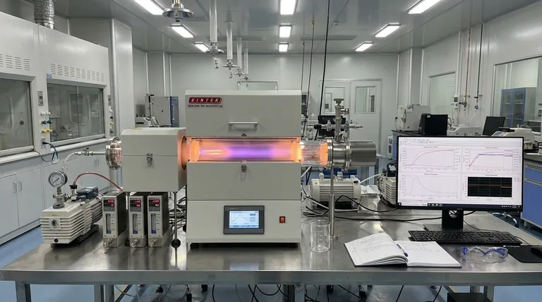
Optimize your PECVD processes with KINTEK's advanced solutions! Leveraging exceptional R&D and in-house manufacturing, we provide diverse laboratories with high-temperature furnace systems like CVD/PECVD Systems, Muffle, Tube, Rotary, Vacuum & Atmosphere Furnaces. Our strong deep customization capability ensures precise alignment with your unique experimental needs, enhancing film quality and efficiency. Contact us today to discuss how we can support your thin film deposition goals!
Visual Guide

Related Products
- Slide PECVD Tube Furnace with Liquid Gasifier PECVD Machine
- RF PECVD System Radio Frequency Plasma Enhanced Chemical Vapor Deposition
- Inclined Rotary Plasma Enhanced Chemical Deposition PECVD Tube Furnace Machine
- Inclined Rotary Plasma Enhanced Chemical Deposition PECVD Tube Furnace Machine
- Multi Heating Zones CVD Tube Furnace Machine for Chemical Vapor Deposition Equipment
People Also Ask
- What are the typical conditions for plasma-enhanced CVD processes? Achieve Low-Temperature Thin Film Deposition
- What plasma source is used in PE-CVD tube furnaces? Unlock Low-Temperature, High-Quality Deposition
- What role does a Tube Furnace play in the CVD growth of carbon nanotubes? Achieve High-Purity CNT Synthesis
- What are the main advantages of PECVD tube furnaces compared to CVD tube furnaces? Lower Temp, Faster Deposition, and More
- How does PECVD equipment contribute to TOPCon bottom cells? Mastering Hydrogenation for Maximum Solar Efficiency


