The primary benefit of using Chemical Vapor Deposition (CVD) with Parylene is the creation of a completely conformal, pinhole-free protective film that cannot be achieved by any other method. This process uniquely enables Parylene's superior properties, providing an ultra-thin barrier against moisture and chemicals, excellent electrical insulation, and robust adhesion to even the most complex surfaces.
The decision to use Parylene is fundamentally a decision to use the CVD process. The material’s exceptional protective qualities are a direct result of how it is applied, making the process and the material inseparable for achieving high-reliability outcomes.

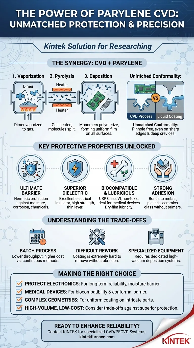
The Synergy of Process and Material
To understand the benefits, you must first understand that Parylene coating is not like painting or dipping. The CVD process is what unlocks the material's full potential by building the coating one molecule at a time directly on the substrate's surface.
How CVD for Parylene Works
The process occurs in a vacuum chamber and consists of three stages. First, the raw, solid Parylene dimer is vaporized into a gas. Second, this gas is heated to a very high temperature (pyrolysis), which splits the molecules into reactive monomers. Finally, these gaseous monomers enter the room-temperature deposition chamber, where they spontaneously polymerize onto every exposed surface, forming a uniform film.
Unmatched Conformality and Uniformity
Because the coating is formed from a gas, it deposits with uniform thickness everywhere. It covers sharp edges, penetrates deep crevices, and coats the inside of tiny tubes without bridging or pooling. This creates a truly pinhole-free encapsulation, which is impossible with liquid coatings that are subject to surface tension.
Precision Control Over Thickness
The CVD process offers exceptional control over film thickness, often down to the sub-micron level. This precision is critical for applications in microelectronics, sensors, and medical devices where tight dimensional tolerances must be maintained.
Key Protective Properties Unlocked by CVD
The unique nature of the CVD process directly translates into a set of powerful material benefits that are ideal for protecting high-value components.
An Ultimate Barrier Against Contaminants
The pinhole-free film created by CVD is a hermetic-quality barrier. It provides robust protection against moisture, corrosive fluids, chemicals, and gases, making it a top choice for electronics and devices operating in harsh environments.
Superior Dielectric Strength
Parylene is an excellent electrical insulator, possessing very high dielectric strength even in a very thin layer. This allows engineers to prevent short circuits and insulate components without adding significant bulk or weight, a critical factor for miniaturization.
Biocompatibility and Dry-Film Lubricity
Parylene is biocompatible (USP Class VI) and non-toxic, making it an industry standard for coating medical implants, surgical tools, and other devices that contact the body. It also provides a dry-film lubricity that can improve the function of moving components.
Strong Adhesion to Diverse Substrates
The deposition process promotes strong molecular bonding. Parylene adheres tenaciously to a wide variety of materials, including metals, plastics, elastomers, ceramics, and glass, often without the need for primers.
Understanding the Trade-offs
While powerful, the CVD process for Parylene is not universally applicable. Its unique nature introduces specific limitations that must be considered.
It Is a Batch Process
Parylene deposition is performed in a vacuum chamber, making it a batch process. This can lead to lower throughput and higher costs compared to continuous liquid coating methods, especially for high-volume consumer goods.
Rework and Removal are Difficult
Once applied, the coating is extremely difficult to remove without physically abrading it or using specialized, aggressive techniques. This makes rework or repair of a coated component a significant challenge.
It Requires Specialized Equipment
Applying Parylene isn't as simple as spraying or dipping. It requires a dedicated, purpose-built CVD vacuum deposition system, representing a significant capital investment and requiring trained operators.
Making the Right Choice for Your Application
Choosing to use Parylene via CVD is a strategic decision based on your primary engineering goal.
- If your primary focus is protecting sensitive, high-value electronics: The combination of a pinhole-free moisture barrier and high dielectric strength is unparalleled for ensuring long-term reliability.
- If your primary focus is medical device biocompatibility: The USP Class VI rating, combined with a completely conformal barrier, makes it an essential technology for implants and critical-contact devices.
- If your primary focus is coating complex geometries: CVD is the only method that ensures a truly uniform film on intricate parts with sharp edges, deep recesses, or internal bores.
- If your primary focus is high-volume, low-cost production: You must carefully weigh the superior protection against the higher processing costs and batch-based throughput of the CVD method.
Ultimately, choosing CVD for Parylene is a decision to prioritize maximum protection, precision, and reliability for your most critical components.
Summary Table:
| Benefit | Description |
|---|---|
| Conformal Coating | Uniform, pinhole-free film covering complex shapes and crevices |
| Moisture and Chemical Barrier | Hermetic-quality protection against harsh environments |
| Electrical Insulation | High dielectric strength for preventing short circuits |
| Biocompatibility | USP Class VI rated, ideal for medical implants and devices |
| Strong Adhesion | Bonds well to various substrates without primers |
| Precision Thickness Control | Sub-micron level accuracy for tight tolerances |
Ready to enhance your product's reliability with advanced Parylene CVD coatings? At KINTEK, we leverage exceptional R&D and in-house manufacturing to provide diverse laboratories with tailored high-temperature furnace solutions, including our specialized CVD/PECVD Systems. Our strong deep customization capability ensures we precisely meet your unique experimental needs for electronics, medical devices, and more. Contact us today to discuss how our expertise can deliver superior protection and performance for your critical components!
Visual Guide
Related Products
- HFCVD Machine System Equipment for Drawing Die Nano Diamond Coating
- Cylindrical Resonator MPCVD Machine System for Lab Diamond Growth
- Custom Made Versatile CVD Tube Furnace Chemical Vapor Deposition CVD Equipment Machine
- RF PECVD System Radio Frequency Plasma Enhanced Chemical Vapor Deposition
- 915MHz MPCVD Diamond Machine Microwave Plasma Chemical Vapor Deposition System Reactor
People Also Ask
- What is Hot-filament Chemical Vapor Deposition (HFCVD)? Achieve High-Quality Thin Films with Precision Control
- What materials are commonly used in CVD coating systems? Explore Key Materials for Superior Coatings
- What is the significance of the vacuum pressure control system in the CVD coating process for powders?
- What core function does CVD equipment serve in h-BN anti-corrosion? Master Precision Synthesis for High-Performance Films
- What are the equipment for chemical vapor deposition? A Guide to the 5 Essential Components


