At its core, Chemical Vapor Deposition (CVD) offers a powerful set of advantages centered on its ability to create highly pure, uniform, and precisely controlled thin films on a wide variety of surfaces. Unlike physical deposition methods that spray material onto a surface, CVD grows a film from chemical precursors, allowing it to coat complex shapes evenly and produce materials with exceptional quality, making it indispensable in fields from microelectronics to advanced materials.
The fundamental advantage of CVD is not just layering a material, but engineering a new surface from the atomic level up. It transforms a passive substrate into a functional component by growing a high-purity film that conforms perfectly to its geometry.
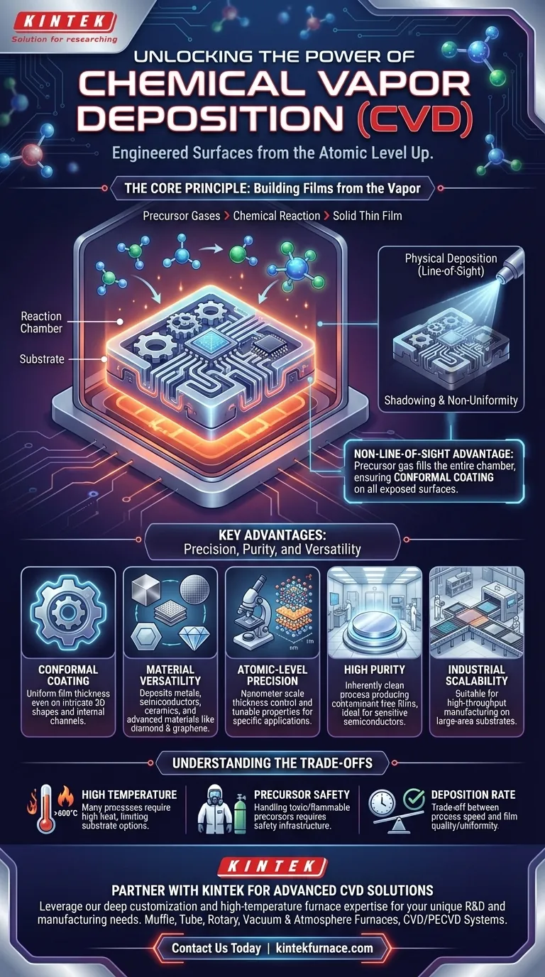
The Core Principle: Building Films from the Vapor Up
To understand the advantages of CVD, you must first grasp how it works. It is fundamentally a process of synthesis, not just application.
What is Chemical Vapor Deposition?
CVD involves introducing one or more volatile precursor gases into a reaction chamber containing the object to be coated, known as the substrate. Energy, typically in the form of high heat, is applied to the system.
This energy causes the precursor gases to react or decompose near the substrate. The solid byproducts of this chemical reaction then deposit onto the substrate, gradually building a thin, solid film.
The "Non-Line-of-Sight" Advantage
Because the precursor is a gas, it fills the entire reaction chamber and surrounds the substrate from all angles. The chemical reaction and subsequent deposition occur on every exposed surface.
This non-line-of-sight characteristic is a critical advantage. It allows CVD to produce a highly conformal coating, meaning the film has a uniform thickness even on complex, three-dimensional shapes with internal channels or intricate features.
Key Advantages in Detail
The principles of gas-phase reaction and uniform deposition give rise to CVD's primary benefits.
Unmatched Material Versatility
By carefully selecting precursor gases and reaction conditions, CVD can deposit an exceptionally wide range of materials. This includes metals, semiconductors, ceramics like silicon nitride, and even advanced carbon forms like diamond and graphene. This makes it a go-to process for creating functional protective coatings against corrosion and wear.
Atomic-Level Precision and Control
CVD provides exceptional control over the final film. Engineers can precisely regulate the film's thickness down to the nanometer scale by adjusting deposition time, gas concentrations, and temperature. Furthermore, the composition and microstructure of the film can be finely tuned to achieve specific electrical, optical, or mechanical properties.
Exceptional Purity and Quality
Building a film from gaseous chemical precursors is an inherently clean process. It results in films of very high purity, free from the contaminants often present in bulk materials. This purity is non-negotiable for applications like semiconductor manufacturing, where even trace impurities can ruin a microchip.
Industrial Scalability
While it is a highly precise process, CVD is not limited to laboratories. The technology is highly scalable for industrial production, capable of coating large-area substrates (like silicon wafers or architectural glass) and enabling high-throughput manufacturing.
Understanding the Trade-offs
No process is without its limitations. Objectivity requires acknowledging the challenges associated with CVD.
High-Temperature Requirements
Many CVD processes, particularly thermal CVD, require very high temperatures (often >600°C) to drive the necessary chemical reactions. This can limit the types of substrates that can be used, as materials with low melting points or temperature sensitivity may be damaged.
Precursor Chemistry and Safety
The "chemical" in CVD involves handling precursor gases that can be highly toxic, flammable, or corrosive. This necessitates significant investment in safety infrastructure, gas handling systems, and exhaust treatment, adding to the operational complexity and cost.
Deposition Rate vs. Quality
While CVD can achieve high deposition rates for some materials, there is often a trade-off between speed and film quality. Processes optimized for the highest-purity, most uniform films are often slower, which can impact throughput for applications requiring very thick coatings.
Making the Right Choice for Your Goal
Selecting CVD depends entirely on your project's technical requirements.
- If your primary focus is fabricating complex micro-devices: CVD's atomic-level precision and exceptional purity are essential for creating reliable transistors and integrated circuits.
- If your primary focus is coating intricate 3D parts: CVD's non-line-of-sight capability ensures complete and uniform coverage where other methods would fail.
- If your primary focus is creating high-performance materials: CVD offers the unique versatility to deposit specialized, high-purity films like synthetic diamond, silicon carbide, or graphene.
Ultimately, the power of Chemical Vapor Deposition lies in its ability to fundamentally engineer a material's surface for performance.
Summary Table:
| Advantage | Description |
|---|---|
| Conformal Coating | Uniform film thickness on complex 3D shapes due to non-line-of-sight deposition. |
| Material Versatility | Deposits metals, semiconductors, ceramics, and advanced materials like diamond and graphene. |
| Atomic-Level Precision | Nanometer-scale thickness control and tunable film properties for specific applications. |
| High Purity | Clean process producing contaminant-free films, ideal for sensitive uses like semiconductors. |
| Industrial Scalability | Suitable for high-throughput manufacturing on large-area substrates. |
Unlock the full potential of Chemical Vapor Deposition for your lab! Leveraging exceptional R&D and in-house manufacturing, KINTEK provides diverse laboratories with advanced high-temperature furnace solutions. Our product line, including Muffle, Tube, Rotary Furnaces, Vacuum & Atmosphere Furnaces, and CVD/PECVD Systems, is complemented by our strong deep customization capability to precisely meet unique experimental requirements. Contact us today to discuss how our tailored CVD systems can enhance your material engineering and production efficiency!
Visual Guide
Related Products
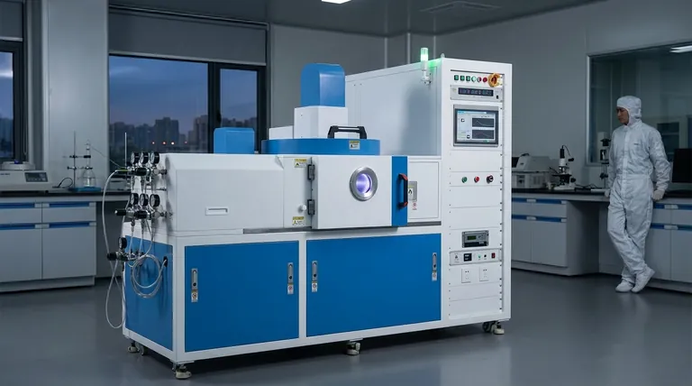
- Custom Made Versatile CVD Tube Furnace Chemical Vapor Deposition CVD Equipment Machine
- RF PECVD System Radio Frequency Plasma Enhanced Chemical Vapor Deposition
- MPCVD Machine System Reactor Bell-jar Resonator for Lab and Diamond Growth
- 915MHz MPCVD Diamond Machine Microwave Plasma Chemical Vapor Deposition System Reactor
- Slide PECVD Tube Furnace with Liquid Gasifier PECVD Machine
People Also Ask
- What are the key features of CVD tube furnaces for 2D material processing? Unlock Precision Synthesis for Superior Materials
- What customization options are available for CVD tube furnaces? Tailor Your System for Superior Material Synthesis
- What is a CVD tube furnace and what is its primary function? Discover Precision Thin-Film Deposition
- What are the practical applications of gate media prepared by CVD tube furnaces? Unlock Advanced Electronics and More
- What future trends are expected in the development of CVD tube furnaces? Discover Smarter, More Versatile Systems


