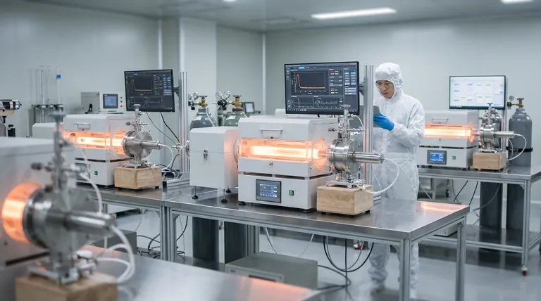
In advanced manufacturing, Plasma-Enhanced Chemical Vapor Deposition (PECVD) is a cornerstone technology used to create critical components in semiconductors, modern displays like OLEDs, solar cells, and medical devices. Its unique ability to deposit exceptionally high-quality thin films at low temperatures makes it indispensable for fabricating products that cannot withstand the high heat of traditional deposition methods.
The central advantage of PECVD is not just what it creates, but how it creates it. By using a plasma to energize chemical reactions, it enables the growth of dense, uniform, and precisely controlled material layers at temperatures low enough to protect sensitive underlying substrates.
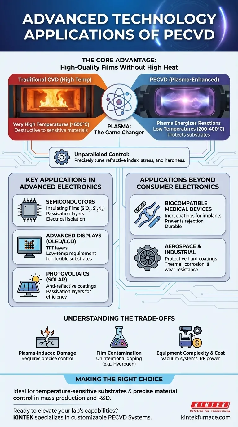
The Core Advantage: High-Quality Films Without High Heat
Traditional Chemical Vapor Deposition (CVD) requires very high temperatures to break down precursor gases and deposit a film. This works for robust materials but is destructive to complex electronics or plastics.
How Plasma Changes the Game
PECVD bypasses the need for intense heat by using a plasma—an energized state of gas. This plasma provides the energy needed for the chemical reactions to occur, allowing deposition to happen at much lower temperatures (typically 200-400°C).
This single factor is what unlocks its use in so many advanced fields.
Unparalleled Control Over Film Properties
Beyond low temperature, PECVD offers a high degree of control. By precisely tuning gas mixtures, pressure, and plasma power, engineers can dictate material properties like refractive index, internal stress, and hardness.
This molecular-level control is essential for optimizing the performance of optical coatings, semiconductors, and protective layers.
Key Applications in Advanced Electronics
The most significant impact of PECVD is in the fabrication of electronic devices, where layers of different materials must be built up without damaging the delicate circuitry already present.
Semiconductor Manufacturing
PECVD is fundamental to modern integrated circuits. It is used to deposit insulating (dielectric) films like silicon dioxide (SiO₂) and silicon nitride (Si₃N₄).
These films are critical for electrically isolating conductive layers, forming capacitors, and providing passivation—a final protective layer that shields the chip from moisture and contaminants. It is also used for creating structures like shallow trench and sidewall isolation.
Advanced Display Technology (OLED & LCD)
Modern high-resolution displays rely on a grid of Thin-Film Transistors (TFTs) to control each individual pixel. PECVD is the primary method for depositing the active and insulating layers that form these transistors.
Because the underlying glass or plastic substrates in OLED and flexible displays are sensitive to heat, PECVD's low-temperature capability is not just an advantage; it is a requirement.
Photovoltaics and Solar Cells
Efficiency in solar cells depends on maximizing light absorption and minimizing electron loss. PECVD is used to deposit anti-reflective coatings that help capture more photons and passivation layers that prevent energy loss at the silicon surface.
The ability to create highly uniform, pure films over large surface areas makes PECVD a cost-effective and efficient solution for solar panel manufacturing.
Applications Beyond Consumer Electronics
PECVD's versatility extends to industries where material durability and unique properties are paramount.
Biocompatible Medical Coatings
Medical implants, such as stents, artificial joints, and surgical tools, must be biocompatible and durable. PECVD can apply thin, inert coatings that prevent rejection by the body and improve wear resistance.
The low-temperature process ensures the underlying implant material is not compromised during coating.
Protective Aerospace and Industrial Coatings
In aerospace and other demanding industrial environments, components are exposed to extreme temperatures and corrosive elements. PECVD is used to apply hard, dense coatings that provide thermal, corrosion, and wear resistance.
Its ability to uniformly coat complex geometries ensures even the most intricate parts are protected.
Understanding the Trade-offs
While powerful, PECVD is not a universal solution. It's essential to understand its limitations.
Plasma-Induced Damage
The same high-energy plasma that enables low-temperature deposition can, if not carefully controlled, cause damage to the substrate surface. This requires sophisticated process control to mitigate.
Film Contamination
The precursor gases used in PECVD often contain hydrogen or other elements that can become incorporated into the deposited film. While sometimes desirable, this unintentional doping can alter the film's electrical or optical properties if not managed.
Equipment Complexity and Cost
PECVD systems, which require vacuum chambers, gas handling systems, and RF power sources to generate plasma, are significantly more complex and expensive than some alternative coating methods.
Making the Right Choice for Your Goal
Selecting a deposition method depends entirely on the technical and economic requirements of your project.
- If your primary focus is mass-producing integrated circuits or displays: PECVD is the established industry standard for depositing high-quality insulating and active films on temperature-sensitive substrates.
- If your primary focus is coating temperature-sensitive or complex-shaped parts: PECVD's combination of low-temperature processing and excellent conformity is ideal for materials that cannot tolerate thermal stress.
- If your primary focus is developing next-generation photovoltaics or optical devices: The precise, molecular-level control PECVD offers over film purity, density, and refractive index is critical for maximizing device performance.
Ultimately, PECVD empowers engineers to build advanced devices that would be impossible to fabricate with high-temperature methods alone.
Summary Table:
| Application Area | Key PECVD Uses | Core Benefits |
|---|---|---|
| Semiconductors | Insulating films (SiO₂, Si₃N₄), passivation layers | Low-temperature processing, precise control, high uniformity |
| Displays (OLED/LCD) | Thin-film transistor layers | Protects heat-sensitive substrates, enables flexible displays |
| Solar Cells | Anti-reflective coatings, passivation layers | Improves light absorption, reduces energy loss |
| Medical Devices | Biocompatible coatings for implants | Enhances durability, prevents rejection, low-temperature safe |
| Aerospace/Industrial | Protective coatings for extreme environments | Provides corrosion, wear, and thermal resistance |
Ready to elevate your lab's capabilities with advanced PECVD solutions? KINTEK specializes in high-temperature furnace technologies, including our state-of-the-art CVD/PECVD Systems. Leveraging exceptional R&D and in-house manufacturing, we offer deep customization to precisely meet your unique experimental needs—whether you're in semiconductor fabrication, display production, solar energy, or medical device development. Contact us today to discuss how our tailored PECVD systems can drive innovation and efficiency in your projects!
Visual Guide
Related Products
- Slide PECVD Tube Furnace with Liquid Gasifier PECVD Machine
- RF PECVD System Radio Frequency Plasma Enhanced Chemical Vapor Deposition
- Inclined Rotary Plasma Enhanced Chemical Deposition PECVD Tube Furnace Machine
- Inclined Rotary Plasma Enhanced Chemical Deposition PECVD Tube Furnace Machine
- Multi Heating Zones CVD Tube Furnace Machine for Chemical Vapor Deposition Equipment
People Also Ask
- What are the typical conditions for plasma-enhanced CVD processes? Achieve Low-Temperature Thin Film Deposition
- What role does a Tube Furnace play in the CVD growth of carbon nanotubes? Achieve High-Purity CNT Synthesis
- How does PECVD equipment contribute to TOPCon bottom cells? Mastering Hydrogenation for Maximum Solar Efficiency
- What is plasma in the context of PECVD? Unlock Low-Temperature Thin Film Deposition
- How does a hydrogen reduction environment in an industrial tube furnace facilitate gold-copper alloy microspheres?


