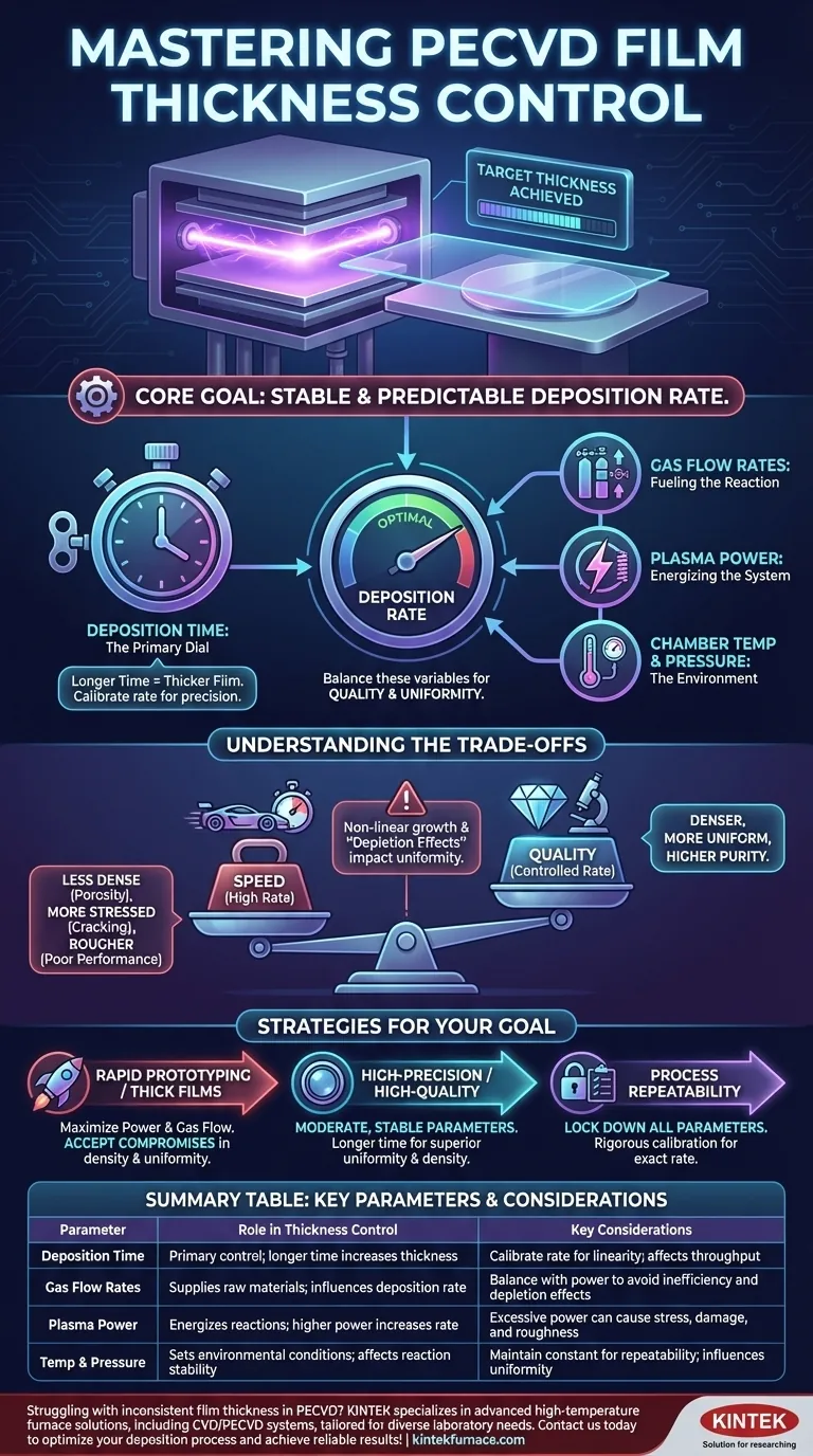
At its core, film thickness in Plasma-Enhanced Chemical Vapor Deposition (PECVD) is controlled by deposition time. This is the primary lever you will use; a longer deposition time generally results in a thicker film. However, achieving a precise, uniform, and high-quality film requires a more nuanced approach where time is balanced with other critical process parameters like gas flow and plasma power.
While deposition time sets the film's final thickness, the true goal is to establish a stable and predictable deposition rate. This rate is a function of multiple variables—gas flow, plasma power, and temperature—which must be carefully balanced to ensure not just thickness, but also film quality and uniformity.
The Core Levers of Thickness Control
To achieve a target thickness, you must first understand the parameters that define your deposition rate. Each one plays a distinct role in the chemical and physical processes happening inside the chamber.
Deposition Time: The Primary Dial
This is the most direct control you have. Once you establish a stable deposition rate for a given set of conditions, the final thickness is a straightforward function of time.
To achieve a specific thickness, you first perform a calibration run for a set duration, measure the resulting film, and then calculate the deposition rate (e.g., in nanometers per minute).
Gas Flow Rates: Fueling the Reaction
The flow rate of precursor gases into the chamber determines the amount of raw material available for deposition.
Increasing the gas flow can increase the deposition rate, but only up to a point. If other parameters like plasma power are not increased accordingly, the excess gas will simply be pumped out without reacting, leading to inefficiency.
Plasma Power: Energizing the System
Plasma power dictates how effectively the precursor gases are dissociated into the reactive species needed for film growth.
Higher power generally increases the deposition rate by creating more reactive ions and radicals. However, excessive power can also lead to film stress, ion bombardment damage, and increased roughness.
Chamber Temperature and Pressure: The Environment
Temperature influences the surface mobility of deposited atoms and the chemical reaction pathways on the substrate. Pressure affects the plasma density and the mean free path of reactive species.
While less commonly used for real-time control, these parameters are foundational to the process recipe. They must be held constant to ensure a stable and repeatable deposition rate.
Understanding the Trade-offs
Simply maximizing the deposition rate is rarely the best strategy. High-quality film deposition is an exercise in managing competing factors.
The Myth of Perfect Linearity
The relationship between deposition time and thickness is not always perfectly linear. An initial nucleation phase at the start of the process can have a different rate than the subsequent bulk growth.
For this reason, short depositions may not scale predictably to very long ones. Always calibrate your rate using a deposition time that is reasonably close to your target process time.
Rate vs. Quality
There is an inherent trade-off between deposition speed and film quality. Aggressively increasing gas flow and plasma power to achieve a high rate can result in films that are:
- Less Dense: With higher porosity or lower refractive index.
- More Stressed: Leading to cracking or poor adhesion.
- Rougher: Impacting optical or electrical performance.
Slower, more controlled depositions often yield denser, more uniform, and higher-purity films.
The Challenge of Uniformity
The settings that control rate also impact thickness uniformity across the substrate. High gas flows can lead to a "depletion effect," where the film is thicker near the gas inlet and thinner downstream.
Similarly, non-uniformities in the plasma itself will be directly imprinted onto the film's thickness profile. Achieving wafer-scale uniformity often requires careful showerhead design and process tuning.
How to Achieve Your Desired Thickness
Your approach should be dictated by your end goal. The right process is the one that meets your specific requirements for precision, quality, and throughput.
- If your primary focus is rapid prototyping or thick films: You can use higher plasma power and gas flow rates to maximize the deposition rate, but be prepared to accept potential compromises in film density and uniformity.
- If your primary focus is high-precision, high-quality films (e.g., optical coatings, semiconductors): Use moderate, stable parameters and a longer deposition time. This slow, controlled growth yields superior uniformity, density, and lower stress.
- If your primary focus is process repeatability: Lock down every parameter—power, temperature, pressure, and gas flows—and perform rigorous calibration runs to determine the exact deposition rate for your recipe.
By moving from simply adjusting time to mastering the entire system of variables, you gain true control over your thin-film deposition process.
Summary Table:
| Parameter | Role in Thickness Control | Key Considerations |
|---|---|---|
| Deposition Time | Primary control; longer time increases thickness | Calibrate rate for linearity; affects throughput |
| Gas Flow Rates | Supplies raw materials; influences deposition rate | Balance with power to avoid inefficiency and depletion effects |
| Plasma Power | Energizes reactions; higher power increases rate | Excessive power can cause stress, damage, and roughness |
| Temperature & Pressure | Sets environmental conditions; affects reaction stability | Maintain constant for repeatability; influences uniformity |
Struggling with inconsistent film thickness in your PECVD processes? KINTEK specializes in advanced high-temperature furnace solutions, including CVD/PECVD systems, tailored for diverse laboratory needs. With our strong R&D and in-house manufacturing, we offer deep customization to precisely meet your unique experimental requirements—ensuring superior control, uniformity, and quality. Contact us today to optimize your deposition process and achieve reliable results!
Visual Guide
Related Products
- RF PECVD System Radio Frequency Plasma Enhanced Chemical Vapor Deposition
- Slide PECVD Tube Furnace with Liquid Gasifier PECVD Machine
- Inclined Rotary Plasma Enhanced Chemical Deposition PECVD Tube Furnace Machine
- Inclined Rotary Plasma Enhanced Chemical Deposition PECVD Tube Furnace Machine
- Cylindrical Resonator MPCVD Machine System for Lab Diamond Growth
People Also Ask
- How does film quality compare between PECVD and CVD? Choose the Best Method for Your Substrate
- What are the advantages of PECVD in film deposition? Achieve Low-Temp, High-Quality Coatings
- How is silicon dioxide deposited from tetraethylorthosilicate (TEOS) in PECVD? Achieve Low-Temperature, High-Quality SiO2 Films
- What is the role of RF power in PECVD and how does the RF-PECVD process work? Master Thin Film Deposition Control
- What are the applications of plasma enhanced chemical vapor deposition? Key Uses in Electronics, Optics & Materials


