At its core, Thermal Chemical Vapor Deposition (CVD) is a manufacturing process that uses high temperatures to initiate chemical reactions in the gas phase, resulting in the creation of a solid, high-performance thin film on a target surface. Precursor gases, which contain the elements of the desired film, are introduced into a heated chamber where they decompose and react, depositing a uniform and highly pure coating onto a substrate.
Thermal CVD is not a simple coating method; it is a precise chemical construction process. High heat acts as the critical energy source that breaks down specific gases, allowing them to rebuild as a solid, engineered film on a substrate's surface.
The Fundamental Principle: Building from Gas
To understand how Thermal CVD works, you must first understand its three primary components: the precursor, the substrate, and the energy source (heat). These elements interact in a controlled environment to build the film layer by layer.
The Precursor Gases: The Building Blocks
Precursor gases are the raw materials for the film. These are carefully selected chemical compounds that are gaseous at or near room temperature but contain the atoms needed for the final solid coating.
For example, to deposit a silicon nitride film, gases like silane (SiH₄) and ammonia (NH₃) might be used as precursors.
The Substrate: The Foundation
The substrate is the material or object onto which the film is deposited. This could be a silicon wafer for a microchip, a glass pane for an optical lens, or a metal part needing a protective layer.
The substrate is placed inside the reaction chamber and heated to the required process temperature.
The Heat: The Catalyst for Reaction
Heat is the engine of Thermal CVD. Temperatures, often ranging from several hundred to over a thousand degrees Celsius, provide the necessary thermal energy to break the chemical bonds within the precursor gas molecules.
This decomposition and subsequent reaction are what allow the desired solid material to form and bond with the substrate surface.
The Four Stages of Deposition
The actual film growth in a Thermal CVD process occurs in a precise, four-stage sequence. This cycle repeats continuously to build the film to its target thickness.
Stage 1: Transport to the Surface
Precursor gases are introduced into the reaction chamber. They must then diffuse through a boundary layer—a thin, stagnant layer of gas—to reach the surface of the heated substrate.
Stage 2: Adsorption
Once the precursor molecules reach the substrate, they land and temporarily stick to its surface. This process is known as adsorption.
Stage 3: Surface Chemical Reaction
This is the critical deposition step. The intense heat of the substrate provides enough energy for the adsorbed molecules to react, either with each other or by decomposing on their own.
This reaction forms the desired solid material, which creates a strong chemical bond with the substrate surface. The film begins to grow.
Stage 4: Desorption of By-products
The chemical reactions that form the solid film also create unwanted gaseous by-products. These by-products must detach from the surface (desorption) and be transported away by the gas flow, exiting through the chamber's exhaust system.
Understanding the Trade-offs
While powerful, Thermal CVD is not a universal solution. Its primary strengths are directly linked to its most significant limitations, and understanding this balance is key to using it effectively.
Pro: Unmatched Film Quality and Purity
The high temperatures used in Thermal CVD result in films that are dense, highly pure, and have excellent adhesion to the substrate. The process produces conformal coatings, meaning it can uniformly cover complex, non-flat surfaces.
Con: The High Temperature Requirement
The reliance on high heat is the single biggest constraint. These temperatures can damage or destroy substrates that are not thermally robust, such as plastics, polymers, or electronic devices with low melting-point metals.
Con: Inefficient Precursor Use
Because the chemical reactions are activated by heat, deposition doesn't just happen on the substrate. It also occurs on the chamber walls and any other heated surface, leading to wasted precursor material and requiring frequent chamber cleaning.
Is Thermal CVD Right for Your Application?
Choosing a deposition method requires aligning the process capabilities with your primary goal.
- If your primary focus is maximum film purity and density for robust applications: Thermal CVD is often the superior choice, provided your substrate can withstand the high process temperatures.
- If your primary focus is coating temperature-sensitive materials (like plastics or complex electronics): You must explore lower-temperature alternatives, such as Plasma-Enhanced CVD (PECVD), which uses plasma instead of high heat to drive the reaction.
- If your primary focus is simple protective coating without stringent purity needs: Other methods like Physical Vapor Deposition (PVD) or even thermal spray might be more cost-effective and faster.
By understanding these core principles, you can select a deposition strategy based on fundamental chemistry and material science, ensuring the best outcome for your project.
Summary Table:
| Aspect | Key Details |
|---|---|
| Process Principle | Uses high temperatures to decompose precursor gases, forming solid films on substrates via chemical reactions. |
| Primary Components | Precursor gases (e.g., SiH₄, NH₃), substrate (e.g., silicon wafers), and heat (up to 1000°C+). |
| Deposition Stages | 1. Transport to surface, 2. Adsorption, 3. Surface reaction, 4. Desorption of by-products. |
| Advantages | High film purity, density, adhesion, and conformal coating on complex shapes. |
| Limitations | Requires high temperatures (can damage sensitive substrates), inefficient precursor use, and frequent cleaning. |
| Ideal Applications | Robust materials needing high-performance coatings; not for temperature-sensitive substrates like plastics. |
Need a reliable high-temperature furnace for your Thermal CVD processes? KINTEK specializes in advanced solutions tailored to your lab's unique requirements. With exceptional R&D and in-house manufacturing, we offer products like Muffle, Tube, Rotary, Vacuum & Atmosphere Furnaces, and CVD/PECVD Systems, all backed by deep customization capabilities. Whether you're working with semiconductors, optics, or protective coatings, our furnaces ensure precise temperature control and uniform heating for superior thin film deposition. Contact us today to discuss how we can enhance your research and production efficiency!
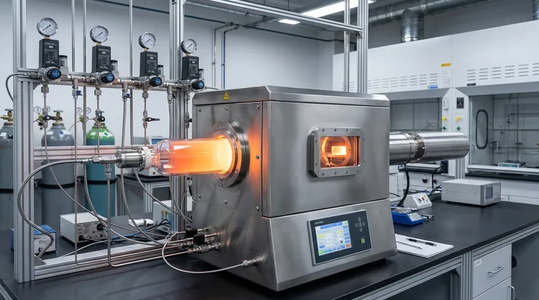
Visual Guide

Related Products
- HFCVD Machine System Equipment for Drawing Die Nano Diamond Coating
- Multi Heating Zones CVD Tube Furnace Machine for Chemical Vapor Deposition Equipment
- Custom Made Versatile CVD Tube Furnace Chemical Vapor Deposition CVD Equipment Machine
- Slide PECVD Tube Furnace with Liquid Gasifier PECVD Machine
- MPCVD Machine System Reactor Bell-jar Resonator for Lab and Diamond Growth
People Also Ask
- What is the significance of the vacuum pressure control system in the CVD coating process for powders?
- How can customers maximize the quality of CVD coatings? Master Pre-Coating Prep for Superior Results
- What are the equipment for chemical vapor deposition? A Guide to the 5 Essential Components
- What is Hot-filament Chemical Vapor Deposition (HFCVD)? Achieve High-Quality Thin Films with Precision Control
- What is chemical vapor deposition (CVD) and its primary industrial application? Unlock Precision Thin Films for Electronics


