The high-temperature thermal profile acts as the master control program for a ceramic's functional destiny. During sintering, the applied heat doesn't just harden the material; it orchestrates atomic diffusion to build and refine the interface between every particle. This directly defines the grain boundary geometry, which governs how electrical charges navigate the material, ultimately setting critical parameters like dielectric constant, resistivity, and breakdown strength.
The core challenge of sintering electroceramics is managing a fundamental conflict: densification versus grain growth. The thermal profile—specifically ramp rate, peak temperature, and dwell time—is the primary tool for tipping this balance. Getting it right creates a network of precisely engineered intergrain contacts, transforming a compacted powder into a functional component with predictable, optimized microelectric properties.
The Foundational Link: Microstructure and Electrical Response
The functional properties of advanced ceramics don't emerge from the bulk grains alone but from the engineered interfaces between them. Your thermal profile is the tool that sculpts this critical landscape.
Why the Grain Boundary Region Dictates Electrical Performance
In many electroceramics, the grain boundary behaves entirely differently from the grain interior. For example, in a varistor or barrier layer capacitor, you have semiconducting grains separated by insulating grain boundaries. The overall electrical response is not a simple average; it's a "grain boundary effect" where these interfaces form a network of back-to-back electrical barriers.
The high-temperature dwell creates these distinct regions. It allows for controlled diffusion of dopants or the formation of secondary phases exactly at the triple points and grain boundaries. The thermal profile's stability during this phase is non-negotiable. A temperature fluctuation can cause a non-uniform boundary phase, creating a weak point that catastrophically degrades the component's breakdown voltage.
The Critical Competition: Densification vs. Coarsening
This is the central dynamic you must master. When you apply heat, two things happen simultaneously:
- Densification: Pores shrink and are eliminated, bringing particle centers closer together and expanding the intergrain contact area.
- Coarsening (Grain Growth): The average grain size increases as larger grains consume smaller ones, reducing total grain boundary energy.
These two processes compete. Densification creates functional, high-contact-area interfaces. Uncontrolled coarsening can destroy them. If grain boundaries migrate too fast during rapid grain growth, they can detach from the pores, trapping them inside the grains. A pore isolated miles away from a grain boundary is impossible to eliminate, limiting your final density and leaving a void that disrupts the local electric field.
How the Thermal Profile Engineers Intergrain Contacts
You are essentially using time and temperature to choreograph atomic motion. The goal is to maximize the formation of clean, high-contact-area interfaces while suppressing the processes that would degrade them.
The Onset of Contact: The Role of Heating Rate
A fast initial heating rate up to the isothermal hold temperature can be a powerful kinetic tool. The driving force for densification is surface energy, which is much smaller than that for grain growth. However, the mobility of the atoms is the common limiting factor.
By using a rapid heating rate, you can hit a high target temperature quickly. This brings the material to a regime of high atomic mobility while the surface area—and thus the densification driving force—is still very high. This tactic can selectively activate densification mechanisms before significant grain growth has a chance to begin, creating a foundation of strong intergrain necks early in the cycle.
Perfecting the Junction: The Role of the Isothermal Hold
The peak temperature and the dwell time at that temperature are where the intergrain contact area is finalized. This is the stage where a compact of particles becomes a single, monolithic body. Thermal energy drives neck formation between adjacent ceramic particles, expanding the contact surface area through vacancy diffusion.
For a given temperature, the equilibrium contact geometry is defined by the balance of surface and grain boundary energies. A precise isothermal hold at, say, 1300°C, allows the system to approach this equilibrium uniformly. This uniformity is everything. It ensures that the resulting grain boundary characteristics, and therefore the permittivity and dielectric loss you measure, are consistent across the entire macroscopic component.
When Contacts Degrade: The Pitfalls of Overtreatment
Pushing the temperature too high or holding for too long triggers grain boundary breakaway. The microstructure becomes a less-than-ideal network. You face two specific failures:
- Pore Detachment: As described, pores become intragranular, creating internal stress concentrators and electrical defects.
- Abnormal Grain Growth: A few grains grow exponentially, creating a duplex structure. This non-uniform microstructure leads to highly scatter-prone and unpredictable electrical properties because the effective insulating grain boundary network is no longer homogeneous.
Understanding the Trade-offs and Paradoxes
The relationship between your thermal profile, the final microstructure, and electrical performance is not always linear. This is where deep understanding separates a functional component from a failed experiment.
The Grain Size Paradox in Dielectrics
A fascinating paradox emerges in materials like BaTiO3-based capacitors. The fundamental physics would predict that the dielectric constant increases as grain size is refined down to approximately 1 µm. This is a core principle for maximizing capacitance.
However, obtaining these ultra-fine grains requires a lower sintering temperature or shorter dwell time. The trade-off is that this may prevent full densification, leaving residual porosity. A pore has a dielectric constant of ~1, which dramatically lowers the overall permittivity of the composite material. Your thermal profile must therefore find the sweet spot: the lowest temperature and shortest time that achieves >98% theoretical density while pinning the grain size at the target 1 µm benchmark. This requires precise control to prevent the grain boundary breakaway that would occur if you tried to eliminate the last 2% of porosity with more heat.
The Hardness-Electrical Property Divergence
A thermal profile optimized for structural properties like micro-indentation hardness might be detrimental to electrical performance. High hardness often correlates with fine grain size and high density, a structure you achieve with a rapid, lower-temperature cycle.
However, certain electroceramics like PTC thermistors require a specific grain boundary oxygen adsorption layer or a secondary phase to function. This often demands a slightly higher thermal budget or a controlled cooling cycle to allow for segregation and defect chemistry equilibration at the grain boundaries. Your target application must dictate the thermal profile; you are not simply maximizing density, but engineering a specific grain-boundary-dependent functional property.
Making the Right Choice for Your Goal
Your optimal thermal profile is a direct function of the macro-property you aim to achieve. The same furnace is a fundamentally different tool based on what you tell it to do.
- If your primary focus is maximizing dielectric constant: Target a profile that yields the finest possible uniform grain size while still achieving >97% density. This likely involves a fast heating rate and a carefully limited dwell at a peak temperature that pins grain growth near the 1 µm threshold, accepting the risk of minimal residual porosity over grain coarsening.
- If your primary focus is optimizing breakdown strength and varistor properties: Prioritize uniform, controlled grain growth to create a perfectly homogeneous network of grain boundary barriers. Your profile should use a stable, precise isothermal hold to ensure every grain boundary junction experiences the same thermal history, eliminating weak spots that would fail under surge conditions.
- If your primary focus is piezoelectric performance: A high degree of densification is non-negotiable to ensure mechanical integrity under cyclic loading, but a fine grain size is often needed to restrict domain wall motion and provide a hard piezoelectric response. Your thermal cycle must be aggressively optimized for densification, potentially using a two-step sintering profile to hit a high temperature briefly before lowering to a long, lower-temperature hold that arrests grain growth while eliminating surface porosity.
Your furnace's ability to provide stable, repeatable thermal profiles transforms ceramic processing from an art into a rigorous science, giving you the power to convert the invisible dynamics of atomic diffusion into a tangible, functional, and profitable electrical performance.
Summary Table:
| Thermal Profile Parameter | Microstructural Effect | Impact on Microelectric Properties |
|---|---|---|
| Rapid Heating Rate | Promotes early densification; suppresses premature grain coarsening | Maintains fine grain structure and high intergrain contact area |
| Isothermal Hold | Drives vacancy diffusion and equilibrium neck formation | Optimizes dielectric constant, permittivity, and uniformity |
| Overtreatment (Thermal Excess) | Causes pore detachment and abnormal grain growth (AGG) | Creates electrical defects, lowering breakdown strength |
| Tailored Cooling Cycle | Facilitates grain boundary segregation and oxygen adsorption | Establishes back-to-back electrical barriers (varistor/PTC) |
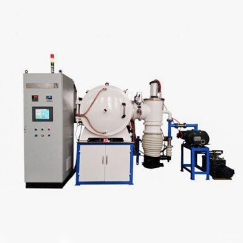
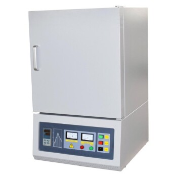
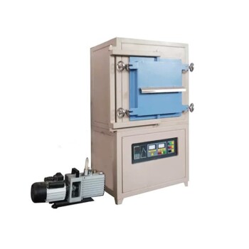
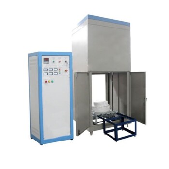
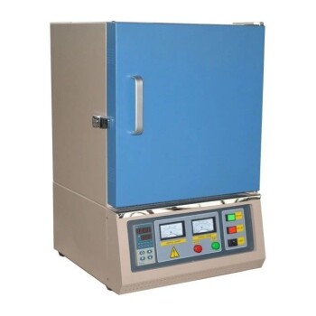
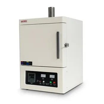
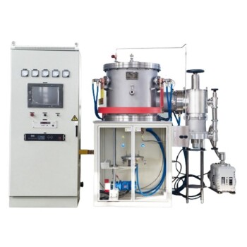
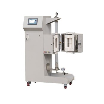
Master your electroceramic sintering profiles with precision-engineered equipment from KINTEK. Specializing in high-performance laboratory equipment and consumables, KINTEK offers a comprehensive line of customizable high-temperature furnaces—including muffle, tube, rotary, vacuum, CVD, and controlled atmosphere systems. Prevent thermal fluctuations, achieve optimal densification, and engineer exact grain boundary properties for your advanced ceramics. Contact KINTEK today to discover our custom thermal solutions!
Related Products
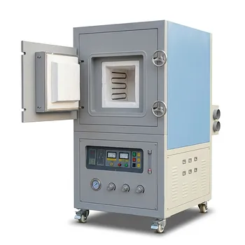
- High Temperature Muffle Oven Furnace for Laboratory Debinding and Pre Sintering
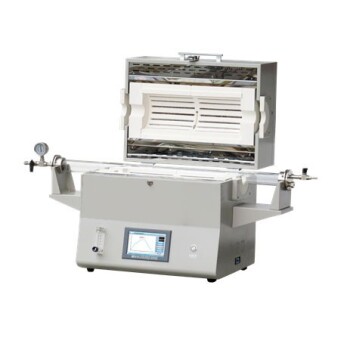
- 1400℃ High Temperature Laboratory Tube Furnace with Alumina Tube
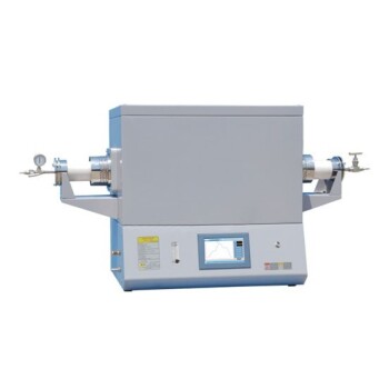
- 1700℃ High Temperature Laboratory Tube Furnace with Alumina Tube
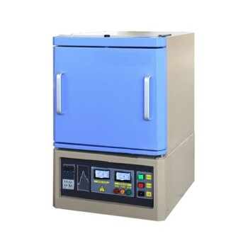
- 1800℃ High Temperature Muffle Oven Furnace for Laboratory
- 2200 ℃ Graphite Vacuum Heat Treat Furnace
People Also Ask
- What thermal phenomena occur during polymer binder burnout in ceramic green bodies? Lab Furnace Guide
- What role does a high-temperature muffle furnace play in STFO synthesis? Achieve Pure Perovskite Results
- Why is controlled heat treatment in a muffle furnace necessary for calcined clay? Achieve Optimal Pozzolanic Activity
- How does a high-temperature muffle furnace facilitate the formation of LaNbxAl1−xO3+δ perovskite structures? Key Roles
- What role does a high-temperature muffle furnace play in the formation of biochar catalysts? Master Catalyst Synthesis