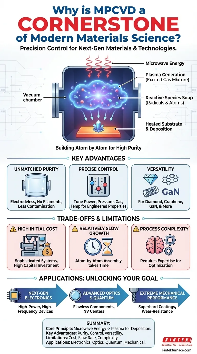
At its core, Microwave Plasma Chemical Vapor Deposition (MPCVD) is a cornerstone of modern materials science because it provides an unparalleled level of control for creating high-purity, high-quality crystalline materials, most notably synthetic diamond. This precision enables the fabrication of components for next-generation electronics, optics, and quantum technologies that would otherwise be impossible to produce.
The true significance of MPCVD is not just its ability to deposit thin films, but its power to engineer material properties at the atomic level. It transforms materials with theoretical promise, like diamond, into practical components that drive technological innovation.
What is MPCVD? A Primer on the Process
To understand why MPCVD is so critical, you must first understand how it works. Unlike other deposition methods, it leverages a clean, efficient energy source to create materials with extreme precision.
The Core Principle: Using Microwaves to Create Plasma
MPCVD uses microwave energy—the same fundamental energy used in a household microwave oven, but far more focused and powerful—to excite a mixture of gases within a vacuum chamber.
This intense energy strips electrons from the gas atoms, creating a plasma. This plasma is an energized cloud of ions, electrons, and reactive neutral species, often described as the fourth state of matter.
The Role of Plasma: A "Soup" of Reactive Species
This plasma is a highly reactive environment. For diamond growth, precursor gases like methane (a carbon source) and hydrogen are introduced.
Inside the plasma, these gases break down into their constituent atoms and radicals (e.g., atomic hydrogen and methyl radicals, CH₃). This "soup" of reactive species is the key to the entire process.
The Deposition Process: Building Atom by Atom
These reactive species then diffuse toward a heated substrate (a small seed crystal or wafer) placed within the chamber.
On the substrate surface, a complex chemical reaction occurs. The carbon-containing radicals bond to the substrate, extending its crystal lattice, while the atomic hydrogen selectively etches away any non-diamond carbon (like graphite), ensuring a pure, high-quality crystal grows layer by layer.
The Key Advantages That Define MPCVD's Importance
The unique mechanism of MPCVD provides several distinct advantages over other synthesis techniques, such as Hot Filament CVD (HFCVD) or High-Pressure/High-Temperature (HPHT) methods.
Unmatched Purity and Quality
Because the plasma is generated by external microwaves, there are no internal electrodes or filaments inside the reaction chamber. This "electrodeless" nature is a critical advantage, as it eliminates a major source of contamination that can plague other methods, leading to exceptionally pure materials.
Precise Control Over Growth Conditions
Operators can independently and precisely tune key process parameters: microwave power, gas pressure, gas composition, and substrate temperature. This fine-grained control allows for the deliberate engineering of a material's properties, from its crystal orientation to its electronic and optical characteristics.
Versatility for Advanced Materials
While most famously used for diamond, MPCVD is a versatile platform for growing other advanced materials, including graphene, carbon nanotubes, and other hard semiconductor materials like Gallium Nitride (GaN). This adaptability makes it a vital tool for materials research and development.
Understanding the Trade-offs and Limitations
No technology is without its compromises. Acknowledging the limitations of MPCVD is crucial for objective assessment.
High Initial Equipment Cost
MPCVD systems are complex machines requiring sophisticated microwave generators, vacuum systems, and process controls. This results in a high capital investment compared to simpler deposition techniques.
Relatively Slow Growth Rates
The atom-by-atom assembly that ensures high quality also means that growth rates can be slower than bulk synthesis methods like HPHT. For applications that require large volumes of lower-grade material (e.g., industrial abrasives), other methods are often more economical.
Process Complexity
The high degree of control is a double-edged sword. Optimizing a process for a specific material or application requires deep expertise and significant process development time. It is not a "plug-and-play" technology.
How to Apply This to Your Goal
The decision to leverage MPCVD depends entirely on what you need to achieve. Its value is unlocked when the demand for material performance justifies the investment in its precision.
- If your primary focus is next-generation electronics: MPCVD is essential for fabricating high-purity, single-crystal diamond wafers for high-power and high-frequency semiconductor devices.
- If your primary focus is advanced optics or quantum computing: The method's control over purity is non-negotiable for creating flawless optical components and nitrogen-vacancy (NV) center diamonds for quantum sensing.
- If your primary focus is extreme mechanical performance: MPCVD enables the deposition of superhard diamond coatings that dramatically extend the life and performance of cutting tools and wear-resistant components.
Ultimately, MPCVD serves as the critical bridge between the theoretical potential of advanced materials and their real-world application in breakthrough technologies.
Summary Table:
| Aspect | Details |
|---|---|
| Core Principle | Uses microwave energy to create plasma for precise material deposition in a vacuum chamber. |
| Key Advantages | Unmatched purity (no electrode contamination), precise control over growth conditions, versatility for materials like diamond, graphene, and GaN. |
| Limitations | High initial equipment cost, relatively slow growth rates, and process complexity requiring expertise. |
| Applications | Next-generation electronics, advanced optics, quantum computing, and extreme mechanical performance coatings. |
Unlock the Power of MPCVD for Your Laboratory
At KINTEK, we understand that achieving high-purity, high-quality materials is essential for driving innovation in fields like electronics, optics, and quantum technologies. Leveraging our exceptional R&D and in-house manufacturing, we provide diverse laboratories with advanced high-temperature furnace solutions tailored to your needs. Our product line, including Muffle, Tube, Rotary Furnaces, Vacuum & Atmosphere Furnaces, and CVD/PECVD Systems, is complemented by strong deep customization capabilities to precisely meet your unique experimental requirements.
Whether you're developing next-generation devices or enhancing material performance, our expertise in MPCVD and related technologies can help you overcome challenges and accelerate your research. Contact us today to discuss how we can support your goals with reliable, customized solutions!
Visual Guide
Related Products
- 915MHz MPCVD Diamond Machine Microwave Plasma Chemical Vapor Deposition System Reactor
- MPCVD Machine System Reactor Bell-jar Resonator for Lab and Diamond Growth
- Cylindrical Resonator MPCVD Machine System for Lab Diamond Growth
- Multi Heating Zones CVD Tube Furnace Machine for Chemical Vapor Deposition Equipment
- Inclined Rotary Plasma Enhanced Chemical Deposition PECVD Tube Furnace Machine
People Also Ask
- How does the MPCVD process work to deposit diamond? A Guide to High-Purity Synthesis
- What are some key features and benefits of the microwave plasma chemical vapor deposition system? Achieve Unmatched Material Synthesis
- What are the main components of an MPCVD machine? Unlock the Secrets of Diamond Synthesis
- What is the MPCVD method and why is it considered effective for diamond deposition? Superior Purity & High Growth Rates
- What is the basic principle of operation for the microwave plasma chemical vapor deposition system? Unlock High-Purity Material Growth


