The definitive answer is that neither PVD nor CVD is universally "better." The superior method depends entirely on your specific application's requirements for film properties, geometry, and material. Physical Vapor Deposition (PVD) excels at creating highly pure, dense, and durable coatings on relatively simple surfaces. In contrast, Chemical Vapor Deposition (CVD) is the superior choice for creating exceptionally uniform and conformal layers over complex, three-dimensional geometries.
The choice between PVD and CVD is not about picking a winner, but about matching the deposition mechanism to your project's most critical outcome. You must decide if your priority is the physical transfer of a pure material (PVD) or a chemically-reacted, perfectly conforming film (CVD).

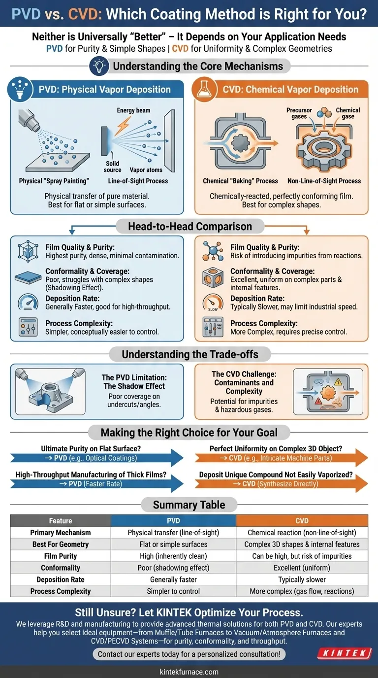
Understanding the Core Mechanisms
To make an informed decision, you must first understand how fundamentally different these two processes are. They are not interchangeable; they are distinct tools for different tasks.
PVD: A Physical "Spray Painting" Process
Think of Physical Vapor Deposition (PVD) as a highly sophisticated form of spray painting in a vacuum. A solid source material is vaporized through physical means (like heating or ion bombardment). This vapor then travels in a straight line through a high-vacuum chamber and condenses onto the substrate, forming a thin film.
The key takeaway is that this is a line-of-sight process. The atoms or molecules of the coating material travel directly from the source to the target.
CVD: A Chemical "Baking" Process
Chemical Vapor Deposition (CVD), on the other hand, is like baking a cake. Precursor gases containing the desired elements are introduced into a reaction chamber. Heat or pressure causes these gases to react on the substrate's surface, "building" the desired film atom by atom as a byproduct of the chemical reaction.
This is a non-line-of-sight process. Because the deposition happens from a gas phase, it can uniformly coat all exposed surfaces, including complex shapes and internal features.
PVD vs. CVD: A Head-to-Head Comparison
Each mechanism's nature creates distinct advantages and disadvantages across several critical performance metrics.
Film Quality and Purity
PVD starts with a highly pure solid material and simply transfers it to the substrate. This makes it an inherently clean process, excellent for applications demanding the highest purity and density with minimal contamination.
CVD relies on chemical reactions, which can sometimes leave behind residual chemicals or byproducts in the film. While high purity is achievable with precise process control and pure precursors, there is a greater inherent risk of introducing impurities.
Conformality and Coverage
This is the most significant point of divergence. CVD excels at conformality, meaning it can produce a film of uniform thickness over complex, non-flat geometries, and even inside deep trenches or holes.
PVD's line-of-sight nature means it struggles with complex shapes. Areas not directly facing the source material will receive little to no coating, creating a "shadowing" effect. It is best suited for flat or gently curved surfaces.
Deposition Rate and Speed
PVD processes generally offer faster deposition rates than CVD. This makes PVD more suitable for applications requiring thick films or high-throughput manufacturing where speed is a critical factor.
CVD is typically a slower process, which can be a limitation for industrial-scale production that demands rapid turnaround.
Process Complexity
The steps in PVD (vaporization and condensation) are conceptually simpler and often easier to control. The primary variables are temperature, time, and chamber pressure.
CVD is a more complex process to manage. It requires precise control over multiple precursor gas concentrations, flow rates, chamber pressure, and temperature to ensure the correct chemical reaction occurs uniformly.
Understanding the Trade-offs
Choosing a method requires acknowledging its inherent limitations. Your decision must be based on which trade-off is more acceptable for your project.
The PVD Limitation: The Shadow Effect
The primary trade-off with PVD is its poor coverage on complex parts. If your component has undercuts, internal channels, or sharp angles, PVD will not provide a uniform coating. This is a non-negotiable physical constraint of the line-of-sight process.
The CVD Challenge: Contaminants and Complexity
The main trade-off with CVD is the potential for impurities and process defects. The chemical reactions must be perfectly controlled to avoid incorporating unwanted elements from the precursor gases. Furthermore, these gases can be hazardous and require significant safety and handling infrastructure.
The Question of Adhesion and Durability
PVD films are often deposited with high kinetic energy, which can result in very dense films with excellent adhesion and durability.
While CVD films also offer good adhesion, the density and hardness can be more variable and highly dependent on the specific chemical process used.
Making the Right Choice for Your Goal
To select the correct method, align your primary objective with the process best suited to achieve it.
- If your primary focus is ultimate purity and density on a flat or simple surface: PVD is your most direct and reliable path for applications like optical coatings or basic semiconductor layers.
- If your primary focus is a perfectly uniform coating on a complex, 3D object: CVD is the only choice due to its superior conformality, ideal for coating internal pipes or intricate machine parts.
- If your primary focus is high-throughput manufacturing of thick films: PVD's typically faster deposition rate offers a significant advantage for production efficiency.
- If your primary focus is depositing a unique compound not easily vaporized: CVD's use of precursor gases provides more flexibility to synthesize materials directly on the substrate.
By understanding their fundamental differences, you move from asking "which is better?" to knowing "which is right for my goal."
Summary Table:
| Feature | PVD (Physical Vapor Deposition) | CVD (Chemical Vapor Deposition) |
|---|---|---|
| Primary Mechanism | Physical transfer (line-of-sight) | Chemical reaction (non-line-of-sight) |
| Best For Geometry | Flat or simple surfaces | Complex 3D shapes & internal features |
| Film Purity | High (inherently clean process) | Can be high, but risk of impurities |
| Conformality | Poor (shadowing effect) | Excellent (uniform on complex parts) |
| Deposition Rate | Generally faster | Typically slower |
| Process Complexity | Simpler to control | More complex (gas flow, reactions) |
Still Unsure Which Coating Method is Right for Your Project?
At KINTEK, we leverage our exceptional R&D and in-house manufacturing to provide advanced thermal solutions for diverse laboratory and industrial needs. Our expertise extends to supporting both PVD and CVD processes with our high-performance furnaces.
Whether you are coating simple flat substrates or complex 3D components, our team can help you select and customize the ideal equipment—from Muffle and Tube Furnaces to sophisticated Vacuum & Atmosphere Furnaces and CVD/PECVD Systems—to meet your unique requirements for purity, conformality, and throughput.
Let's optimize your deposition process. Contact our experts today for a personalized consultation!
Visual Guide
Related Products
- Custom Made Versatile CVD Tube Furnace Chemical Vapor Deposition CVD Equipment Machine
- Multi Heating Zones CVD Tube Furnace Machine for Chemical Vapor Deposition Equipment
- Split Chamber CVD Tube Furnace with Vacuum Station CVD Machine
- RF PECVD System Radio Frequency Plasma Enhanced Chemical Vapor Deposition
- Slide PECVD Tube Furnace with Liquid Gasifier PECVD Machine
People Also Ask
- How does CVD tube furnace sintering enhance graphene growth? Achieve Superior Crystallinity and High Electron Mobility
- How can integrating CVD tube furnaces with other technologies benefit device fabrication? Unlock Advanced Hybrid Processes
- What improvements can be made to the bonding force of gate dielectric films using a CVD tube furnace? Enhance Adhesion for Reliable Devices
- What are the benefits of developing new precursor materials for CVD tube furnaces? Unlock Advanced Thin-Film Synthesis
- What is the working principle of a CVD tube furnace? Achieve Precise Thin Film Deposition for Your Lab


