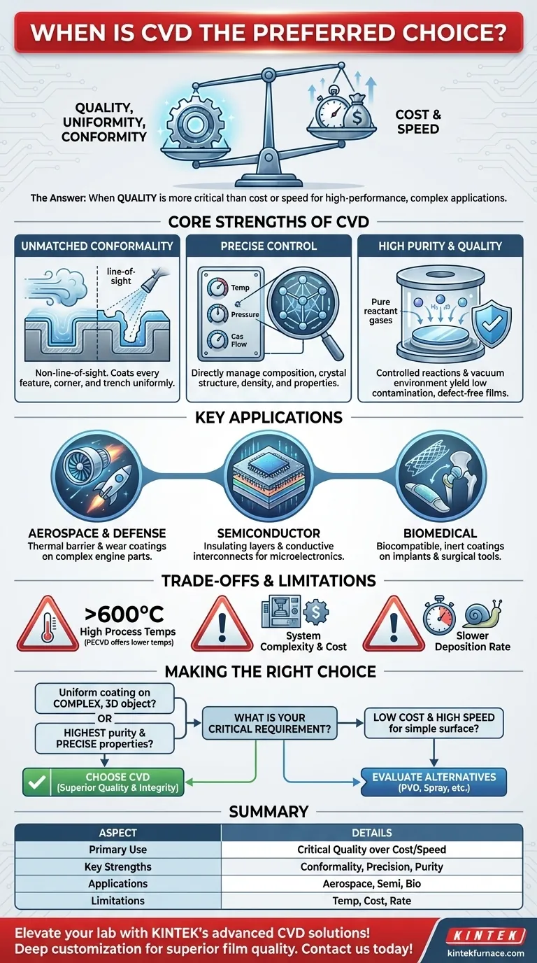
In short, Chemical Vapor Deposition (CVD) is the preferred method when the quality, uniformity, and conformity of a thin film are more critical than the cost or speed of deposition. It excels at creating high-purity, precisely controlled coatings on complex, irregular, or three-dimensional surfaces where other line-of-sight methods would fail.
The core decision to use CVD hinges on a simple trade-off: you are choosing superior film quality and geometric conformity in exchange for potentially higher process complexity and cost. It is the go-to solution for high-performance applications where material integrity is non-negotiable.
The Core Strengths of Chemical Vapor Deposition (CVD)
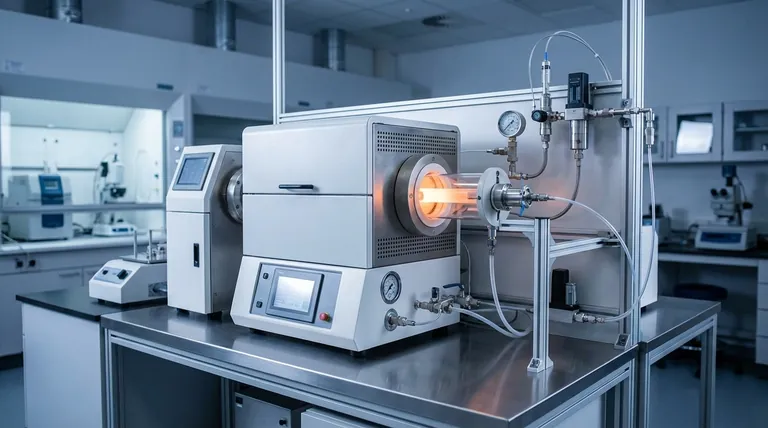
To understand when to choose CVD, you must first grasp its fundamental advantages. The process involves introducing precursor gases into a chamber, which then react and decompose on a heated substrate to form the desired solid film. This gas-phase mechanism is the source of its unique strengths.
Unmatched Conformality on Complex Shapes
CVD is not a "line-of-sight" process like Physical Vapor Deposition (PVD). Because the precursor materials are gases, they can flow into and around every feature of a substrate, no matter how intricate.
This results in a highly conformal coating, meaning the film has a uniform thickness across all surfaces, including sharp corners, deep trenches, and internal cavities. This is impossible to achieve with methods that spray or evaporate material in a straight line.
Precise Control Over Film Properties
The final properties of the deposited film are a direct function of the chemical reaction. By precisely managing variables like substrate temperature, system pressure, and the flow rates of different precursor gases, you gain exceptional control.
This allows you to fine-tune the film's composition, crystal structure, density, and electrical or optical properties to meet exact specifications.
High Purity and Film Quality
The chemical reactions in a CVD process are designed to be highly selective, depositing only the desired material. This, combined with the use of high-purity precursor gases and a controlled vacuum environment, results in films with very low levels of contamination and defects.
This purity is critical for applications in semiconductors and optics, where even minute impurities can degrade performance.
Key Applications Where CVD is Necessary
The strengths of CVD make it the necessary choice in fields where performance and reliability cannot be compromised.
Aerospace and Defense
Components like turbine blades, engine parts, and rocket nozzles are exposed to extreme temperatures and corrosive environments. CVD is used to apply thermal barrier coatings (TBCs) and wear-resistant layers that protect the underlying superalloy. The complex geometry of these parts makes CVD's conformality essential.
Semiconductor Manufacturing
CVD is a cornerstone of modern microelectronics. It is used to deposit a wide range of materials, from the insulating silicon dioxide layers that separate transistors to the conductive tungsten films that form electrical interconnects. The process's precision and purity are paramount for creating reliable, high-density integrated circuits.
Biomedical Devices
Medical implants, surgical tools, and diagnostic sensors often require specialized coatings. CVD can apply biocompatible, inert, or hermetic layers to seal sensitive electronics or prevent adverse reactions with the body. Its ability to uniformly coat the complex shapes of stents or joint replacements is a key advantage.
Understanding the Trade-offs and Limitations
No technology is a universal solution. Being a trusted advisor means acknowledging where CVD may not be the best fit.
High Process Temperatures
Traditional CVD processes often require very high temperatures (often >600°C) to drive the necessary chemical reactions. This can damage or warp temperature-sensitive substrates like polymers or certain metals.
However, variants like Plasma-Enhanced CVD (PECVD) can operate at much lower temperatures, mitigating this issue for many applications.
System Complexity and Cost
A CVD system involves sophisticated vacuum chambers, high-purity gas handling systems, and precise temperature controls. Precursor gases can be toxic, flammable, or corrosive, requiring significant safety infrastructure. This generally makes CVD more complex and expensive to set up and operate than simpler methods like electroplating or spray coating.
Deposition Rate
For applications where the primary goal is to apply a thick, non-critical coating quickly, CVD may not be the most efficient choice. Its deposition rates can be slower than techniques like thermal spray or certain PVD processes.
Making the Right Choice for Your Application
Your decision should be driven by the most critical requirement of your project.
- If your primary focus is coating a complex, 3D object uniformly: CVD is the superior choice due to its non-line-of-sight nature and excellent conformality.
- If your primary focus is achieving the highest purity and precise material properties: CVD offers unparalleled control over the film's chemical composition, density, and crystalline structure.
- If your primary focus is low cost and high speed for a simple, flat surface: You should evaluate alternative methods like PVD, sputtering, or electroplating, which may be more economical.
Ultimately, choosing CVD is a strategic decision to prioritize the quality and integrity of the final film above all other factors.
Summary Table:
| Aspect | Details |
|---|---|
| Primary Use | When film quality, uniformity, and conformity are critical over cost or speed |
| Key Strengths | Unmatched conformality on complex shapes, precise control over film properties, high purity |
| Common Applications | Aerospace (e.g., turbine blades), semiconductors (e.g., insulating layers), biomedical devices (e.g., implants) |
| Limitations | High process temperatures, system complexity and cost, slower deposition rates |
Elevate your lab's capabilities with KINTEK's advanced CVD solutions! Leveraging exceptional R&D and in-house manufacturing, we provide diverse laboratories with high-temperature furnace systems like our CVD/PECVD Systems, Muffle, Tube, Rotary Furnaces, and Vacuum & Atmosphere Furnaces. Our strong deep customization capability ensures precise alignment with your unique experimental needs, delivering superior film quality and performance. Don't compromise on material integrity—contact us today to discuss how we can support your high-performance applications!
Visual Guide
Related Products
- Custom Made Versatile CVD Tube Furnace Chemical Vapor Deposition CVD Equipment Machine
- Multi Heating Zones CVD Tube Furnace Machine for Chemical Vapor Deposition Equipment
- HFCVD Machine System Equipment for Drawing Die Nano Diamond Coating
- Split Chamber CVD Tube Furnace with Vacuum Station CVD Machine
- 915MHz MPCVD Diamond Machine Microwave Plasma Chemical Vapor Deposition System Reactor
People Also Ask
- What are the key features of CVD tube furnaces for 2D material processing? Unlock Precision Synthesis for Superior Materials
- Which industries and research fields benefit from CVD tube furnace sintering systems for 2D materials? Unlock Next-Gen Tech Innovations
- How does CVD tube furnace sintering enhance graphene growth? Achieve Superior Crystallinity and High Electron Mobility
- What customization options are available for CVD tube furnaces? Tailor Your System for Superior Material Synthesis
- What improvements can be made to the bonding force of gate dielectric films using a CVD tube furnace? Enhance Adhesion for Reliable Devices


