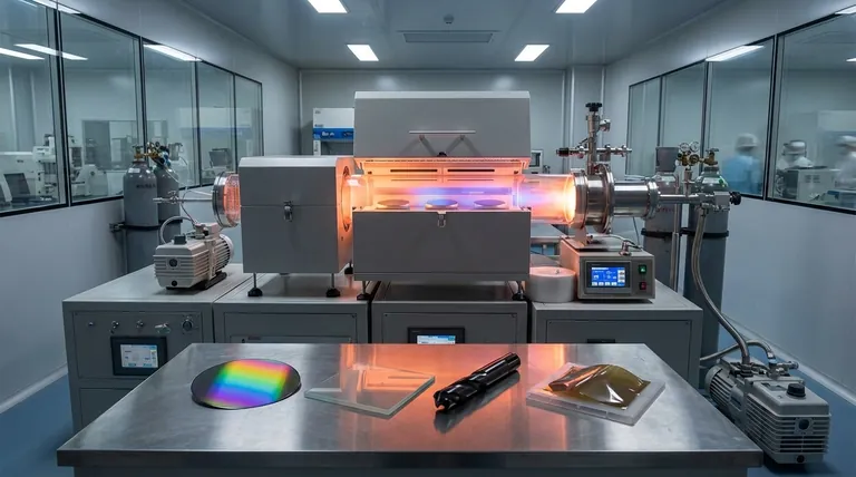
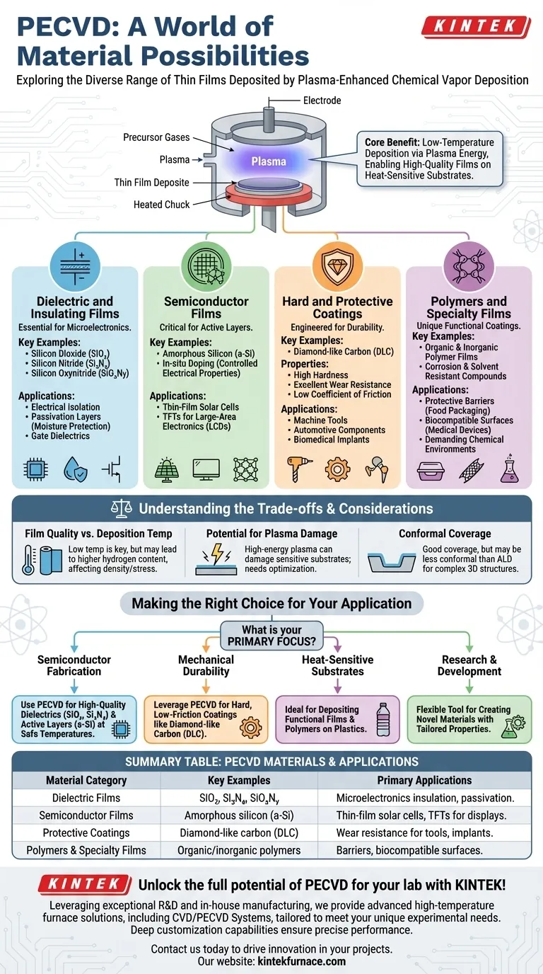
At its core, Plasma-Enhanced Chemical Vapor Deposition (PECVD) is defined by its material versatility. It can deposit a vast range of thin films, most notably essential microelectronic materials like silicon dioxide (SiO₂) and silicon nitride (Si₃N₄), semiconductor layers like amorphous silicon (a-Si), and durable protective coatings such as diamond-like carbon (DLC). This flexibility makes it a foundational process in numerous high-technology fields.
The key to PECVD's versatility is its use of plasma to enable chemical reactions at low temperatures. This unlocks the ability to deposit high-quality films on a wide variety of substrates, including those that cannot tolerate the intense heat of traditional deposition methods.
The Primary Material Categories of PECVD
PECVD is not limited to a single class of material. Its capability extends across insulators, semiconductors, and specialized functional coatings, each serving distinct industrial and scientific purposes.
Dielectric and Insulating Films
These materials are the bedrock of modern microelectronics, used to electrically isolate conductive layers from one another.
The most common PECVD dielectrics are silicon dioxide (SiO₂) and silicon nitride (Si₃N₄). They serve as excellent insulators, passivation layers to protect devices from moisture and contaminants, and gate dielectrics in transistors.
PECVD can also deposit silicon oxynitride (SiOxNy), a film whose properties can be tuned between those of an oxide and a nitride by adjusting the precursor gas ratio.
Semiconductor Films
PECVD is critical for depositing semiconductor materials, particularly where crystalline structures are not required or low temperatures are mandatory.
Amorphous silicon (a-Si) is a primary example, widely used in thin-film solar cells and as the active layer in thin-film transistors (TFTs) for large-area electronics like LCD displays.
A key advantage of the PECVD process is the ability to perform in-situ doping, where dopant gases are introduced during deposition to precisely control the film's electrical properties.
Hard and Protective Coatings
Beyond electronics, PECVD excels at creating films designed for mechanical performance and environmental resistance.
Diamond-like Carbon (DLC) is a category of hard, amorphous carbon films with exceptional properties. These films provide high hardness, excellent wear resistance, and a very low coefficient of friction.
DLC coatings are applied to machine tools, automotive components, and biomedical implants to dramatically increase their lifespan and performance.
Polymers and Specialty Films
The low-temperature nature of PECVD makes it uniquely suitable for depositing polymeric films onto heat-sensitive substrates like plastics.
These organic and inorganic polymer films are used in applications ranging from protective barriers in food packaging to creating biocompatible surfaces on medical devices.
The process is also flexible enough to create unique compounds with high corrosion and solvent resistance, tailored for demanding chemical environments.
Understanding the Trade-offs
While incredibly versatile, PECVD is not a universal solution. Understanding its limitations is crucial for proper application.
Film Quality vs. Deposition Temperature
The primary advantage of PECVD—its low deposition temperature—is also the source of its main trade-off.
Films deposited via PECVD often have a higher concentration of incorporated hydrogen compared to films from high-temperature processes like LPCVD (Low-Pressure CVD). This can impact the film's density, stress, and electrical characteristics.
Potential for Plasma Damage
The high-energy plasma that drives the deposition reaction can sometimes cause physical or electrical damage to the substrate surface.
This is a critical consideration when working with highly sensitive device architectures, and process parameters must be carefully optimized to mitigate this risk.
Conformal Coverage
While PECVD provides good coverage, it may not achieve the same level of conformality—the ability to uniformly coat complex, high-aspect-ratio trenches—as other processes like Atomic Layer Deposition (ALD). This makes it less suitable for certain advanced 3D device structures.
Making the Right Choice for Your Application
Selecting a deposition method depends entirely on your material needs and substrate constraints. PECVD's strength lies in its balance of quality, temperature, and material flexibility.
- If your primary focus is semiconductor fabrication: Use PECVD for high-quality dielectric insulation (SiO₂, Si₃N₄) and active layers (a-Si) at temperatures that protect underlying device structures.
- If your primary focus is mechanical durability: Leverage PECVD to deposit hard, low-friction coatings like Diamond-like Carbon (DLC) on tools, components, or medical implants.
- If your primary focus is heat-sensitive substrates: PECVD is the ideal choice for depositing functional films, including polymers, on plastics or other materials that cannot withstand high heat.
- If your primary focus is research and development: The process's flexibility makes it an exceptional tool for creating and testing novel materials with tailored optical, electrical, or mechanical properties.
Understanding this spectrum of materials is the first step toward leveraging PECVD's unique process advantages for your specific technical goal.
Summary Table:
| Material Category | Key Examples | Primary Applications |
|---|---|---|
| Dielectric Films | SiO₂, Si₃N₄, SiOxNy | Microelectronics insulation, passivation |
| Semiconductor Films | Amorphous silicon (a-Si) | Thin-film solar cells, TFTs for displays |
| Protective Coatings | Diamond-like carbon (DLC) | Wear resistance for tools, implants |
| Polymers & Specialty Films | Organic/inorganic polymers | Barriers, biocompatible surfaces |
Unlock the full potential of PECVD for your lab with KINTEK! Leveraging exceptional R&D and in-house manufacturing, we provide advanced high-temperature furnace solutions, including CVD/PECVD Systems, tailored to meet your unique experimental needs. Whether you're working with dielectrics, semiconductors, or protective coatings, our deep customization capabilities ensure precise performance. Contact us today to discuss how our expertise can enhance your material deposition processes and drive innovation in your projects.
Visual Guide
Related Products
- Slide PECVD Tube Furnace with Liquid Gasifier PECVD Machine
- RF PECVD System Radio Frequency Plasma Enhanced Chemical Vapor Deposition
- Inclined Rotary Plasma Enhanced Chemical Deposition PECVD Tube Furnace Machine
- Inclined Rotary Plasma Enhanced Chemical Deposition PECVD Tube Furnace Machine
- Multi Heating Zones CVD Tube Furnace Machine for Chemical Vapor Deposition Equipment
People Also Ask
- What are the main advantages of PECVD tube furnaces compared to CVD tube furnaces? Lower Temp, Faster Deposition, and More
- What are the typical conditions for plasma-enhanced CVD processes? Achieve Low-Temperature Thin Film Deposition
- What role does a Tube Furnace play in the CVD growth of carbon nanotubes? Achieve High-Purity CNT Synthesis
- How does PECVD equipment contribute to TOPCon bottom cells? Mastering Hydrogenation for Maximum Solar Efficiency
- What are the advantages of using a tube furnace CVD system for Cu(111)/graphene? Superior Scalability and Quality


