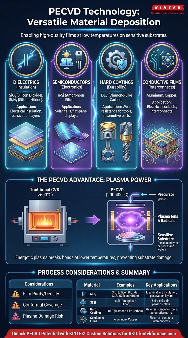
In short, PECVD is a remarkably versatile technology used to deposit a wide array of thin films. The most common materials include silicon compounds like silicon dioxide (SiO₂) for insulation and silicon nitride (SiN) for protection, semiconductors such as amorphous silicon (a-Si) for solar cells, and specialized hard coatings like diamond-like carbon (DLC) for wear resistance. It can also be used for certain metals, polymers, and other advanced composite layers.
The true power of Plasma-Enhanced Chemical Vapor Deposition (PECVD) isn't just the wide range of materials it can deposit, but its ability to do so at significantly lower temperatures than conventional methods. This opens the door for creating high-quality films on temperature-sensitive substrates that would otherwise be damaged.
The Core Material Groups of PECVD
PECVD's utility stems from its ability to create films that serve distinct functions, from electrical insulation to mechanical protection. These materials can be broadly organized into a few key categories.
Dielectrics: The Foundation of Insulation
Dielectric films are electrical insulators, and they represent a primary application of PECVD in the semiconductor industry.
The most common examples are silicon dioxide (SiO₂) and silicon nitride (Si₃N₄). SiO₂ serves as a high-quality insulator between conductive layers, while Si₃N₄ is often used as a durable passivation layer, protecting the sensitive device circuitry from moisture and contamination.
Semiconductors: The Engine of Electronics
PECVD is critical for depositing semiconductor materials, particularly over large areas or on flexible substrates.
Amorphous silicon (a-Si) is a cornerstone material deposited by PECVD. Its application is central to thin-film solar panels (photovoltaics) and the thin-film transistors (TFTs) that control pixels in modern flat-panel displays. More advanced processes can also produce polycrystalline or even epitaxial silicon films.
Hard and Protective Coatings: Enhancing Durability
Beyond electronics, PECVD is a powerful tool for material science, used to create films with exceptional mechanical properties.
Diamond-Like Carbon (DLC) is a key example. These films are extremely hard, chemically inert, and have a very low coefficient of friction. This makes them ideal for protective coatings on cutting tools, automotive engine parts, and biomedical implants to reduce wear and improve longevity.
Conductive Films and Other Materials
While less common than for dielectrics, PECVD can also deposit conductive layers.
This includes metals like aluminum and copper, as well as refractory metals and their silicides, often used for creating electrical contacts or interconnects in specific device architectures. The technology's flexibility also extends to depositing metal oxides, oxynitrides, and even some polymers.
Why Plasma Makes PECVD So Versatile
The secret to PECVD's low-temperature operation and material flexibility lies in its use of plasma. Understanding this principle is key to grasping its advantages over other methods.
Breaking Bonds Without Extreme Heat
Traditional Chemical Vapor Deposition (CVD) relies on very high temperatures (often >600°C) to provide enough thermal energy to break apart precursor gas molecules and initiate a chemical reaction on the substrate surface.
PECVD, by contrast, generates an electromagnetic field to ionize the precursor gases, creating a plasma. This plasma is a highly energetic soup of ions and radicals that are extremely reactive. These radicals can then react and form a film at much lower temperatures, typically in the 200-400°C range.
Enabling Deposition on Sensitive Substrates
This low-temperature process is the defining advantage of PECVD.
It allows for the deposition of high-quality films on substrates that cannot withstand high heat. This includes fully fabricated silicon wafers with existing metal layers, plastics, and other polymers, dramatically expanding the range of possible applications.
Tailoring Film Properties
The plasma environment gives engineers significant control over the final film.
By precisely adjusting process parameters like gas composition, pressure, and plasma power, you can fine-tune the deposited film's properties. This includes its density, internal stress, chemical composition, and optical index, allowing for the customization of films for very specific requirements.
Understanding the Trade-offs
No technology is without its limitations. Being an effective advisor means acknowledging where PECVD might fall short.
Film Purity and Density
Because the deposition occurs at lower temperatures, PECVD films can sometimes incorporate byproducts from the plasma reaction, such as hydrogen. This can result in films that are less dense or pure than those grown with high-temperature methods, which may affect their electrical performance.
Conformal Coverage
PECVD is a directional process, meaning it can sometimes struggle to coat the inside of very deep, narrow trenches or complex 3D structures uniformly. For applications requiring perfect "step coverage," other technologies like Atomic Layer Deposition (ALD) may be superior.
Potential for Plasma Damage
The same energetic plasma that enables low-temperature deposition can, if not properly controlled, cause physical or electrical damage to the substrate surface. This is a known factor that process engineers must carefully manage during recipe development.
Making the Right Choice for Your Goal
Your choice of deposition technology should be driven by the primary requirement of your specific application.
- If your primary focus is high-quality insulation on a temperature-sensitive device: PECVD is an industry standard for depositing silicon dioxide and silicon nitride.
- If your primary focus is creating large-area electronics like solar panels or displays: PECVD's efficiency in depositing amorphous silicon makes it a leading choice.
- If your primary focus is enhancing the surface durability of a mechanical part: PECVD is ideal for applying hard, low-friction coatings like Diamond-Like Carbon (DLC).
- If your primary focus is achieving the absolute highest purity and conformal coverage: You may need to evaluate higher-temperature CVD or Atomic Layer Deposition (ALD) as alternatives.
Understanding these material capabilities and underlying principles empowers you to select the right deposition technology for your specific engineering challenge.
Summary Table:
| Material Category | Common Examples | Key Applications |
|---|---|---|
| Dielectrics | Silicon Dioxide (SiO₂), Silicon Nitride (Si₃N₄) | Electrical insulation, passivation layers |
| Semiconductors | Amorphous Silicon (a-Si) | Solar cells, flat-panel displays |
| Hard Coatings | Diamond-Like Carbon (DLC) | Wear resistance for tools, automotive parts |
| Conductive Films | Aluminum, Copper | Electrical contacts, interconnects |
Unlock the full potential of PECVD for your laboratory needs with KINTEK! Leveraging exceptional R&D and in-house manufacturing, we provide advanced high-temperature furnace solutions, including our specialized CVD/PECVD Systems. Our strong deep customization capability ensures precise alignment with your unique experimental requirements, whether you're working with dielectrics, semiconductors, or protective coatings. Contact us today to discuss how our tailored solutions can enhance your research and development efficiency!
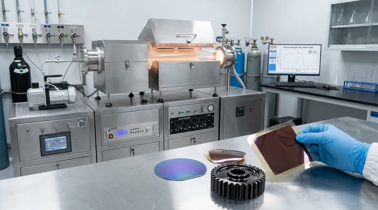
Visual Guide
Related Products
- Slide PECVD Tube Furnace with Liquid Gasifier PECVD Machine
- RF PECVD System Radio Frequency Plasma Enhanced Chemical Vapor Deposition
- Inclined Rotary Plasma Enhanced Chemical Deposition PECVD Tube Furnace Machine
- Inclined Rotary Plasma Enhanced Chemical Deposition PECVD Tube Furnace Machine
- Multi Heating Zones CVD Tube Furnace Machine for Chemical Vapor Deposition Equipment
People Also Ask
- What role does a Tube Furnace play in the CVD growth of carbon nanotubes? Achieve High-Purity CNT Synthesis
- How does a hydrogen reduction environment in an industrial tube furnace facilitate gold-copper alloy microspheres?
- What are the disadvantages of tube furnace cracking when processing heavy raw materials? Avoid Costly Downtime and Inefficiency
- In which industries is the tube furnace commonly used? Essential for Materials Science, Energy, and More
- What is plasma in the context of PECVD? Unlock Low-Temperature Thin Film Deposition


