In short, the most common materials deposited using PECVD are silicon-based dielectrics and semiconductors, such as silicon dioxide (SiO₂), silicon nitride (Si₃N₄), and amorphous silicon (a-Si). However, the technology's true strength lies in its versatility, enabling the deposition of a much wider range of films, including carbon-based layers and even some metals.
The core value of Plasma-Enhanced Chemical Vapor Deposition (PECVD) is not just the list of materials it can deposit, but its ability to do so at significantly lower temperatures than other methods. This single characteristic makes it indispensable for creating complex, multi-layered devices where higher temperatures would damage previously fabricated structures.
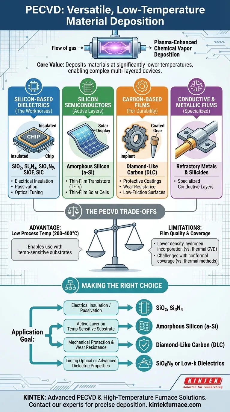
The Core Material Groups in PECVD
While the list of potential films is long, they can be organized into a few key functional categories. Each category serves a distinct purpose in industries ranging from semiconductors to optics.
Silicon-Based Dielectrics: The Workhorses
These films are the foundation of modern microelectronics, primarily serving as insulators and protective layers.
The most frequently used PECVD materials fall into this group, including silicon dioxide (SiO₂) and silicon nitride (Si₃N₄). They are used to electrically isolate conductive layers, act as etch masks, and provide surface passivation.
Specialty dielectrics like silicon oxynitride (SiOxNy) and low-k dielectrics such as SiOF or SiC are also deposited to fine-tune optical properties or reduce parasitic capacitance in high-speed circuits.
Silicon Semiconductors: The Active Layers
PECVD is also critical for depositing silicon films that have active electronic or photovoltaic properties.
Amorphous silicon (a-Si) is a primary example, widely used in thin-film solar cells and as the channel layer in thin-film transistors (TFTs) for large-area displays.
The process can also be tuned to deposit polycrystalline silicon (poly-Si) or even epitaxial silicon, though other methods are often preferred for high-performance crystalline applications.
Carbon-Based Films: For Durability and Beyond
This category highlights PECVD's utility outside of traditional microelectronics.
Diamond-Like Carbon (DLC) is a key material deposited by PECVD. It creates exceptionally hard, low-friction surfaces used for protective coatings on mechanical parts, medical implants, and optical components to enhance wear resistance.
Conductive and Metallic Films: A Specialized Application
While less common than dielectric deposition, PECVD can be used to deposit conductive layers.
This includes films like refractory metals and their silicides. These applications are specialized but demonstrate the process's wide-ranging chemical capabilities.
Understanding the Trade-offs
PECVD is a powerful tool, but its advantages come with specific trade-offs that are critical to understand for any practical application. Its primary benefit—low process temperature—is also the source of its main limitations.
Film Quality vs. Thermal Processes
Because PECVD operates at lower temperatures (typically 200-400°C), the deposited films often have a different structure than those from high-temperature processes like Low-Pressure CVD (LPCVD).
PECVD films may have lower density and incorporate more hydrogen from the precursor gases. This can affect the film's electrical properties, etch rate, and long-term stability, which must be accounted for in device design.
Conformal Coverage
Achieving a perfectly uniform film thickness over complex, high-aspect-ratio topography (known as conformality) can be more challenging with PECVD than with thermal CVD methods.
While process parameters can be heavily optimized to improve step coverage, the directional nature of the plasma can sometimes lead to thicker films on horizontal surfaces than on vertical sidewalls.
Making the Right Choice for Your Application
Selecting the right PECVD material is entirely dependent on your end goal. The process's versatility allows you to choose a film based on the specific electrical, mechanical, or optical properties you need to achieve.
- If your primary focus is electrical insulation and passivation: You will almost certainly use silicon dioxide (SiO₂) for isolation or silicon nitride (Si₃N₄) for a robust moisture and chemical barrier.
- If your primary focus is creating an active semiconductor layer on a temperature-sensitive substrate: Amorphous silicon (a-Si) is the ideal choice for applications like displays or flexible electronics.
- If your primary focus is mechanical protection and wear resistance: Diamond-like carbon (DLC) is the material to specify for creating a hard, durable, and low-friction surface.
- If your primary focus is tuning optical or advanced dielectric properties: You would explore materials like silicon oxynitride (SiOxNy) or low-k dielectrics to meet specific refractive index or capacitance requirements.
Ultimately, understanding these material classes transforms PECVD from a simple deposition tool into a strategic capability for advanced device engineering.
Summary Table:
| Material Category | Key Examples | Primary Applications |
|---|---|---|
| Silicon-Based Dielectrics | SiO₂, Si₃N₄, SiOxNy | Electrical insulation, passivation, optical tuning |
| Silicon Semiconductors | Amorphous Silicon (a-Si) | Thin-film transistors (TFTs), solar cells |
| Carbon-Based Films | Diamond-Like Carbon (DLC) | Protective, wear-resistant coatings |
| Conductive/Metallic Films | Metal Silicides | Specialized conductive layers |
Need a PECVD system tailored to your specific material requirements?
At KINTEK, we leverage our exceptional R&D and in-house manufacturing to provide advanced high-temperature furnace solutions, including our versatile PECVD systems. Our product line is complemented by strong deep customization capabilities to precisely meet your unique experimental and production needs, whether you are working with sensitive semiconductors, durable protective coatings, or specialized optical films.
Contact our experts today to discuss how we can help you achieve precise, low-temperature deposition for your next project.
Visual Guide
Related Products
- RF PECVD System Radio Frequency Plasma Enhanced Chemical Vapor Deposition
- Inclined Rotary Plasma Enhanced Chemical Deposition PECVD Tube Furnace Machine
- Inclined Rotary Plasma Enhanced Chemical Deposition PECVD Tube Furnace Machine
- Slide PECVD Tube Furnace with Liquid Gasifier PECVD Machine
- Vacuum Dental Porcelain Sintering Furnace for Dental Laboratories
People Also Ask
- What is RF in PECVD? A Critical Control for Plasma Deposition
- What are some promising applications of PECVD-prepared 2D materials? Unlock Advanced Sensing and Optoelectronics
- What is the role of RF power in PECVD and how does the RF-PECVD process work? Master Thin Film Deposition Control
- What is PECVD specification? A Guide to Choosing the Right System for Your Lab
- What are the key advantages of PECVD technology? Achieve Low-Temperature, High-Quality Thin Film Deposition