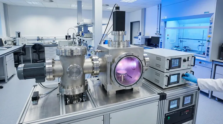
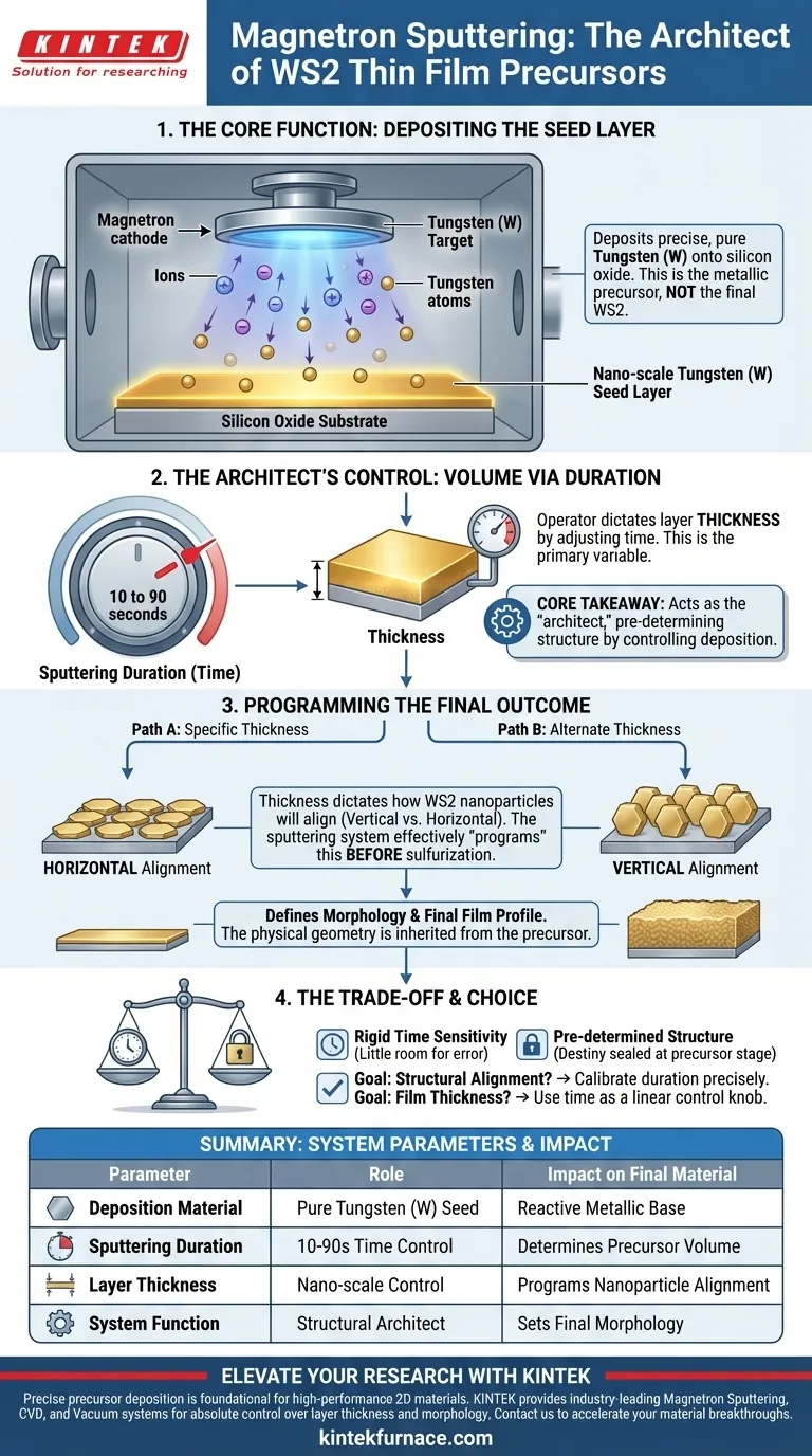
The primary function of a magnetron sputtering system in this context is to deposit a precise, nano-scale tungsten (W) seed layer onto a silicon oxide substrate. This system serves as the foundational manufacturing step, creating the metallic precursor that will eventually be converted into tungsten disulfide (WS2).
Core Takeaway The magnetron sputtering system acts as the "architect" of the final material's structure; by controlling the duration of the tungsten deposition, it pre-determines the thickness, morphology, and physical alignment of the resulting WS2 nanoparticles.
The Role of Deposition in Precursor Formation
Creating the Metallic Seed Layer
The sputtering system is not responsible for creating the compound WS2 directly. Instead, its specific job is to deposit pure tungsten (W) onto a silicon oxide base.
This tungsten layer acts as the "seed" material. It provides the necessary metal atoms that will react during the subsequent sulfurization process.
Controlling Volume via Duration
The system manages the volume of the precursor material through time management. The reference highlights a specific operational window, typically between 10 and 90 seconds.
By adjusting this duration, the operator precisely dictates the thickness of the initial metal layer. This is the primary variable that influences the final product's characteristics.
How Sputtering Influences Final WS2 Properties
Determining Nanoparticle Alignment
The most critical output of the sputtering phase is the orientation of the final material. The thickness of the tungsten seed layer dictates how the WS2 nanoparticles will arrange themselves.
Depending on the thickness achieved during sputtering, the final WS2 particles will align either vertically or horizontally. The sputtering system effectively "programs" this alignment before the chemical reaction even begins.
Defining Morphology and Final Thickness
The physical geometry (morphology) of the final WS2 is inherited from the precursor. The sputtering system establishes the structural baseline that the sulfurization process follows.
Consequently, the final thickness of the WS2 film is a direct result of the initial tungsten deposition. A thicker precursor layer invariably leads to a modified final film profile.
Understanding the Trade-offs
Sensitivity to Sputtering Time
The connection between sputtering duration and material outcome is rigid. Because the system relies on time (10 to 90 seconds) to control thickness, there is little room for error.
Pre-determination of Structure
The trade-off of this method is that the material's destiny is sealed during the precursor stage. You cannot easily alter the alignment (vertical vs. horizontal) during the sulfurization step; it must be correctly defined by the sputtering system first.
Making the Right Choice for Your Goal
To maximize the effectiveness of the magnetron sputtering system, you must reverse-engineer your process based on the desired material properties.
- If your primary focus is specific structural alignment: Calibrate the sputtering duration precisely within the 10-90 second window to target either vertical or horizontal orientation.
- If your primary focus is film thickness: Use the sputtering time as a linear control knob to increase or decrease the volume of the tungsten seed layer.
The magnetron sputtering system is not just a deposition tool; it is the control mechanism that defines the final architecture of your thin film.
Summary Table:
| Parameter | Role in WS2 Preparation | Impact on Final Material |
|---|---|---|
| Deposition Material | Pure Tungsten (W) | Acts as the reactive metallic seed layer |
| Sputtering Duration | 10 to 90 seconds | Directly determines precursor volume and film thickness |
| Layer Thickness | Nano-scale control | Programs vertical vs. horizontal nanoparticle alignment |
| System Function | Structural Architect | Sets the morphology inherited by the final WS2 film |
Elevate Your Thin Film Research with KINTEK
Precise precursor deposition is the foundation of high-performance 2D materials. KINTEK provides industry-leading Magnetron Sputtering, CVD, and Vacuum systems designed to give you absolute control over layer thickness and morphology.
Whether you are developing WS2 semiconductors or advanced nanomaterials, our expert R&D and customizable lab furnaces ensure your research achieves repeatable, high-quality results. Contact KINTEK today to discuss your unique project needs and see how our manufacturing expertise can accelerate your material breakthroughs.
Visual Guide
References
- Thin Films of Tungsten Disulfide Grown by Sulfurization of Sputtered Metal for Ultra-Low Detection of Nitrogen Dioxide Gas. DOI: 10.3390/nano15080594
This article is also based on technical information from Kintek Furnace Knowledge Base .
Related Products
- Cylindrical Resonator MPCVD Machine System for Lab Diamond Growth
- RF PECVD System Radio Frequency Plasma Enhanced Chemical Vapor Deposition
- HFCVD Machine System Equipment for Drawing Die Nano Diamond Coating
- MPCVD Machine System Reactor Bell-jar Resonator for Lab and Diamond Growth
People Also Ask
- Why is temperature control important in the MPCVD growth process? Ensure High-Quality, Reliable Diamond Film Deposition
- What factors influence the quality of diamond deposition in the MPCVD method? Master the Critical Parameters for High-Quality Diamond Growth
- How do carbon-containing groups contribute to diamond growth in the MPCVD method? Unlock High-Quality Diamond Synthesis
- What are the essential components of an MPCVD reactor system? Build a Pristine Environment for High-Purity Materials
- How does pressure affect the MPCVD growth process? Master Plasma Control for Superior Film Quality


