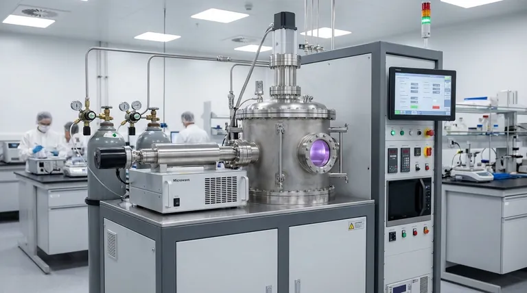
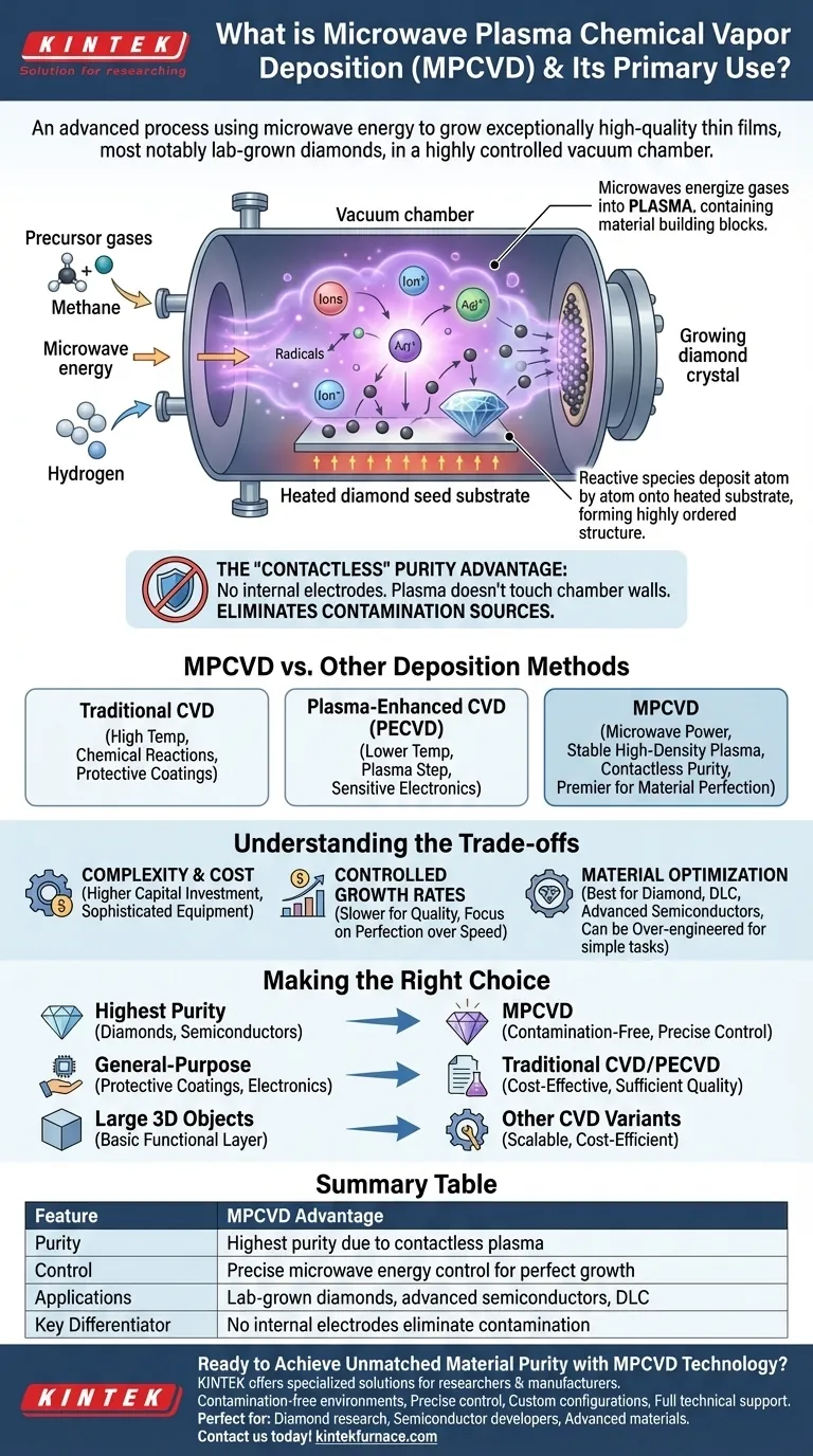
Microwave Plasma Chemical Vapor Deposition (MPCVD) is an advanced process that uses microwave energy to grow exceptionally high-quality thin films, most notably lab-grown diamonds. By energizing precursor gases into a plasma state within a highly controlled vacuum chamber, it enables the precise deposition of materials onto a substrate, atom by atom.
MPCVD's true value lies in its ability to create an ultra-pure, precisely controlled growth environment. By using microwaves to generate a contained plasma, it eliminates the common sources of contamination found in other methods, making it the gold standard for producing high-purity diamond and other advanced materials.
How MPCVD Works: A Matter of Purity and Control
To understand why MPCVD is a game-changer, you must first understand its core mechanism. It isn't just about applying a coating; it's about building a new material from the ground up in the cleanest possible environment.
The Role of Microwaves and Plasma
MPCVD begins with introducing specific precursor gases, such as methane and hydrogen for diamond growth, into a vacuum chamber. Microwave energy is then directed into the chamber, energizing these gases and stripping electrons from their atoms to create plasma—a reactive cloud of ions and radicals.
Creating the Ideal Growth Environment
This plasma cloud contains the fundamental building blocks of the desired material (e.g., carbon atoms for diamond). These reactive species then deposit onto a heated substrate, often a small diamond "seed" crystal, where they arrange themselves into a highly ordered crystalline structure, effectively growing the new material.
The "Contactless" Purity Advantage
The defining feature of MPCVD is its method of plasma generation. Unlike other techniques, there are no internal electrodes inside the chamber. The plasma is generated and contained by the microwave field itself, preventing it from touching the chamber walls.
This "contactless" approach is critical because it eliminates the two main sources of contamination: impurities sputtering off of internal electrodes and contaminants from the chamber walls. The result is a film of exceptionally high purity.
MPCVD vs. Other Deposition Methods: A Critical Distinction
MPCVD is part of a larger family of technologies called Chemical Vapor Deposition (CVD), but its specific use of microwaves gives it unique advantages.
Traditional Chemical Vapor Deposition (CVD)
Traditional CVD uses high temperatures to trigger the chemical reactions needed to deposit a film. It is a robust and widely used process for creating protective coatings and thin films in the semiconductor industry.
The Plasma Enhancement (PECVD)
Plasma-Enhanced CVD (PECVD) adds a plasma generation step to the process. This allows the deposition to occur at much lower temperatures, which is crucial for sensitive electronics. MPCVD is a specialized, high-performance type of PECVD that uses microwaves as its power source.
Why Microwaves are a Game-Changer
While other PECVD methods exist, the use of microwaves generates a more stable, higher-density plasma. This, combined with the contamination-free "contactless" environment, allows for a level of control and purity that other methods cannot easily achieve, making it the premier choice for applications where material perfection is paramount.
Understanding the Trade-offs
No technology is without its compromises. While MPCVD delivers unparalleled quality, it comes with specific considerations.
Complexity and Cost
MPCVD systems are highly sophisticated pieces of equipment. The need for precision microwave generators, advanced vacuum systems, and meticulous gas control makes the initial capital investment significantly higher than for traditional CVD setups.
Controlled Growth Rates
Achieving near-perfect crystal structures requires a deliberate, controlled growth process. Consequently, the deposition rates in MPCVD can be slower than less precise, bulk deposition techniques. The focus is on quality over raw speed.
Material Optimization
MPCVD is heavily optimized for materials where its purity benefits justify the cost, primarily diamond, diamond-like carbon (DLC), and other advanced semiconductors. For simpler coatings where absolute purity is not the primary driver, it can be an over-engineered and less cost-effective solution.
Making the Right Choice for Your Goal
Choosing a deposition technology depends entirely on your specific requirements for material purity, performance, and cost.
- If your primary focus is producing the highest-purity lab-grown diamonds or next-generation semiconductor materials: MPCVD is the undisputed leading choice due to its contamination-free process and precise control.
- If your primary focus is general-purpose protective coatings against corrosion or standard thin films for electronics: Traditional CVD or other PECVD methods often provide a more cost-effective solution with sufficient quality for the task.
- If your primary focus is coating large, complex 3D objects with a basic functional layer: The scalability and cost-efficiency of other CVD variants may be more suitable.
Ultimately, understanding the principle of contamination control is the key to selecting the right tool for your material deposition needs.
Summary Table:
| Feature | MPCVD Advantage |
|---|---|
| Purity | Highest purity due to contactless plasma generation |
| Control | Precise microwave energy control for perfect crystal growth |
| Applications | Lab-grown diamonds, advanced semiconductors, DLC coatings |
| Key Differentiator | No internal electrodes eliminate contamination sources |
Ready to Achieve Unmatched Material Purity with MPCVD Technology?
Leveraging exceptional R&D and in-house manufacturing, KINTEK provides diverse laboratories with advanced high-temperature furnace solutions. Our MPCVD systems are engineered for researchers and manufacturers who demand the highest quality lab-grown diamonds and semiconductor materials.
Our specialized MPCVD solutions offer:
- Contamination-free deposition environments
- Precise microwave plasma control
- Custom configurations for unique research requirements
- Full technical support from installation to operation
Perfect for: Diamond research labs, semiconductor developers, and advanced materials manufacturers.
Contact us today to discuss how our MPCVD technology can elevate your material synthesis capabilities!
Visual Guide
Related Products
- 915MHz MPCVD Diamond Machine Microwave Plasma Chemical Vapor Deposition System Reactor
- MPCVD Machine System Reactor Bell-jar Resonator for Lab and Diamond Growth
- Cylindrical Resonator MPCVD Machine System for Lab Diamond Growth
- RF PECVD System Radio Frequency Plasma Enhanced Chemical Vapor Deposition
- Multi Heating Zones CVD Tube Furnace Machine for Chemical Vapor Deposition Equipment
People Also Ask
- What are the essential components of an MPCVD reactor system? Build a Pristine Environment for High-Purity Materials
- In which industries is the microwave plasma chemical vapor deposition system commonly used? Unlock High-Purity Material Synthesis
- What is the purpose of a microwave plasma chemical vapor deposition system? Grow High-Purity Diamonds and Advanced Materials
- What is the basic principle of operation for the microwave plasma chemical vapor deposition system? Unlock High-Purity Material Growth
- What factors influence the quality of diamond deposition in the MPCVD method? Master the Critical Parameters for High-Quality Diamond Growth


