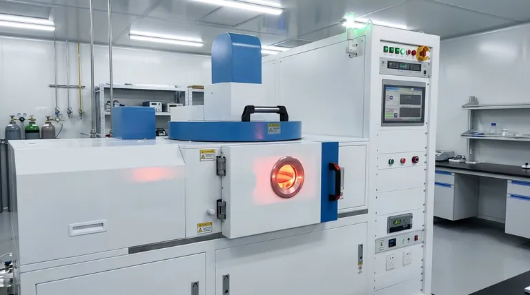
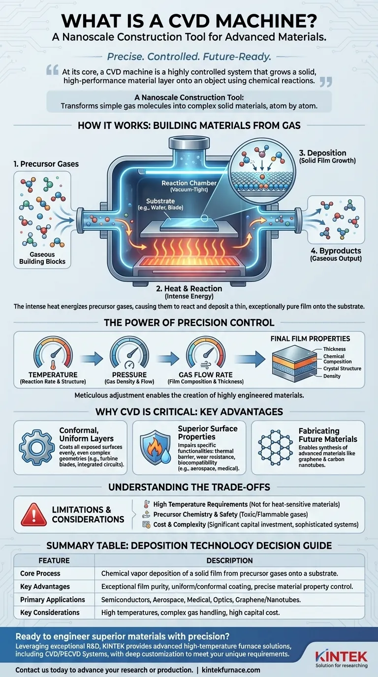
At its core, a CVD machine is a highly controlled system that grows a solid, high-performance material layer onto an object using chemical reactions. Operating under a vacuum, the machine introduces specific gases (precursors) that react and decompose in the heat, depositing a thin, exceptionally pure film onto a substrate. This process is fundamental to the manufacturing of advanced electronics, optics, and protective coatings.
A CVD machine is not simply a coating apparatus; it is a nanoscale construction tool. By precisely manipulating gas chemistry, temperature, and pressure, it transforms simple gaseous molecules into complex, high-performance solid materials directly on a target surface.
How a CVD Machine Builds Materials from Gas
A CVD machine functions like a high-tech oven where chemistry, not just heat, does the work. The entire process is designed for absolute precision and control over the final material.
The Core Components: Chamber, Substrate, and Precursors
Every CVD process involves three key elements. The reaction chamber is a sealed, vacuum-tight vessel that creates a highly controlled environment, free of contaminants.
Inside the chamber sits the substrate, which is the object or material to be coated—such as a silicon wafer, a turbine blade, or a medical implant.
Finally, precursor gases are the chemical building blocks. These are volatile compounds that contain the atoms needed for the final film and are piped into the chamber in precise amounts.
The Deposition Process: From Gas to Solid
The process begins by placing the substrate inside the chamber and creating a vacuum. The chamber and substrate are then heated to a specific, often very high, temperature.
Once the target temperature is reached, the precursor gases are introduced. The intense heat energizes the gas molecules, causing them to break apart and react, either in the gas phase or directly on the substrate's hot surface.
This chemical reaction results in the desired solid material "condensing" or depositing onto the substrate, forming a thin, uniform film. The other byproducts of the reaction remain gaseous and are pumped out of the chamber.
The Power of Precision Control
The defining feature of CVD is its controllability. By meticulously adjusting variables like temperature, pressure, and the flow rate of different precursor gases, operators can dictate the final film's properties.
This allows for exact control over the film's thickness, its chemical composition, its crystal structure, and its density, enabling the creation of highly engineered materials.
Why CVD is a Critical Manufacturing Tool
The ability to build custom materials atom by atom makes CVD indispensable across numerous high-tech industries. Its value lies in creating properties that are impossible to achieve with conventional methods.
Creating Conformal, Uniform Layers
Unlike line-of-sight techniques like spraying, the gases in a CVD process flow around the substrate, coating all exposed surfaces evenly. This results in a conformal film that perfectly covers even the most intricate and complex geometries.
This capability is critical for applications like coating the internal cooling channels of an aerospace turbine blade or ensuring complete coverage on the microscopic structures of an integrated circuit.
Engineering Superior Surface Properties
CVD is used to impart specific functionalities to a material's surface. In the aerospace industry, it creates thermal barrier and wear-resistant coatings that protect components from extreme heat and friction.
In the medical field, it is used to apply biocompatible coatings to implants, improving how they interact with the human body. In optics, it is the standard for producing anti-reflective and other specialized coatings on lenses.
Fabricating the Materials of the Future
CVD is at the forefront of materials science research. It is a key method for synthesizing advanced materials like graphene and carbon nanotubes, which have revolutionary electrical and mechanical properties but are difficult to produce at scale by other means.
Understanding the Trade-offs
While powerful, CVD is not a universal solution. Its operational principles come with inherent limitations that make it unsuitable for certain applications.
High Temperature Requirements
Most CVD processes, particularly thermal CVD, rely on elevated temperatures to drive the chemical reactions. This makes the technique incompatible with substrates that have low melting points or are otherwise sensitive to heat, such as many polymers.
Precursor Chemistry and Safety
The precursor gases used in CVD can often be highly toxic, flammable, or corrosive. This necessitates complex and expensive gas handling and exhaust abatement systems, as well as stringent safety protocols for operators.
Cost and Complexity
CVD machines are sophisticated and expensive to acquire, operate, and maintain. The combination of vacuum systems, high-temperature heating, and precise gas flow control makes them a significant capital investment best suited for high-value applications.
Making the Right Choice for Your Application
Selecting a deposition technology requires matching its capabilities to your specific goal. CVD excels where purity, conformity, and material performance are paramount.
- If your primary focus is creating ultra-pure, dense thin films for electronics or optics: CVD is the industry standard for achieving the required atomic-level control and film quality.
- If your primary focus is adding a functional, high-performance coating to a complex 3D part: CVD's ability to create perfectly conformal layers makes it superior to line-of-sight methods.
- If your primary focus is rapid, low-cost coating on temperature-sensitive materials: You should investigate alternative methods like PVD (Physical Vapor Deposition) or various wet chemical processes, as CVD's heat, cost, and complexity may be prohibitive.
Understanding the principles of CVD empowers you to select the right tool for building materials with precision from the atoms up.
Summary Table:
| Feature | Description |
|---|---|
| Core Process | Chemical vapor deposition of a solid film from precursor gases onto a substrate. |
| Key Advantages | Exceptional film purity, uniform/conformal coating on complex shapes, precise control over material properties. |
| Primary Applications | Semiconductor manufacturing, aerospace coatings, medical implants, optics, synthesis of graphene/nanotubes. |
| Key Considerations | High operating temperatures, complex precursor gas handling, significant capital investment. |
Ready to engineer superior materials with precision?
Leveraging exceptional R&D and in-house manufacturing, KINTEK provides diverse laboratories with advanced high-temperature furnace solutions. Our product line, including Muffle, Tube, Rotary Furnaces, Vacuum & Atmosphere Furnaces, and CVD/PECVD Systems, is complemented by our strong deep customization capability to precisely meet your unique experimental requirements.
Contact us today to discuss how our CVD expertise can advance your research or production.
Visual Guide
Related Products
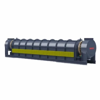
- 915MHz MPCVD Diamond Machine Microwave Plasma Chemical Vapor Deposition System Reactor
- Custom Made Versatile CVD Tube Furnace Chemical Vapor Deposition CVD Equipment Machine
- Cylindrical Resonator MPCVD Machine System for Lab Diamond Growth
- HFCVD Machine System Equipment for Drawing Die Nano Diamond Coating
- Split Chamber CVD Tube Furnace with Vacuum Station CVD Machine
People Also Ask
- What are some key features and benefits of the microwave plasma chemical vapor deposition system? Achieve Unmatched Material Synthesis
- How does the MPCVD process work to deposit diamond? A Guide to High-Purity Synthesis
- What are the essential components of an MPCVD reactor system? Build a Pristine Environment for High-Purity Materials
- What is the basic principle of operation for the microwave plasma chemical vapor deposition system? Unlock High-Purity Material Growth
- What factors influence the quality of diamond deposition in the MPCVD method? Master the Critical Parameters for High-Quality Diamond Growth