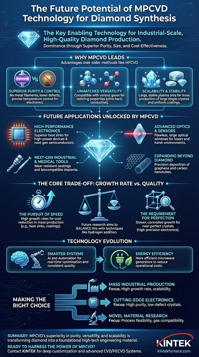
In short, Microwave Plasma Chemical Vapor Deposition (MPCVD) is positioned to be the dominant technology for industrial-scale synthesis of high-quality diamonds. Its future potential lies in its unique ability to mass-produce large, pure, single-crystal diamonds with tailored properties, unlocking next-generation applications in electronics, optics, and advanced materials.
The core takeaway is that MPCVD is not just another method for making diamonds; it is the key enabling technology. Its superiority in controlling purity, size, and cost is what will transition lab-grown diamonds from niche applications to foundational components in mainstream high-tech industries.
Why MPCVD is the Leading Method for Diamond Synthesis
The excitement surrounding MPCVD stems from its fundamental advantages over older methods, such as Hot Filament CVD (HFCVD). These advantages directly address the primary barriers to the widespread use of synthetic diamond.
Superior Purity and Control
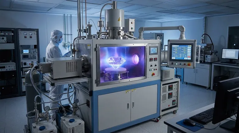
The MPCVD process uses microwave energy to generate plasma, completely avoiding the hot metal filaments used in other techniques. This design is critical because it eliminates the primary source of contamination from materials like tungsten or tantalum.
The result is a diamond with significantly higher purity and fewer defects, which is a non-negotiable requirement for sensitive electronic and optical applications. Furthermore, the process allows for highly stable and precise temperature control, ensuring reproducible quality.
Unmatched Versatility
Unlike filament-based methods that are sensitive to certain gases, MPCVD systems are compatible with a wide range of gas mixtures. This flexibility allows producers to precisely tailor the diamond's properties for different industrial needs, from creating ultra-hard coatings to electrically conductive layers.
Scalability and Stability
MPCVD technology generates a large and stable plasma area. This is the key to growing larger single-crystal diamonds and coating large substrates, such as silicon wafers, uniformly. This inherent scalability makes it the most promising method for cost-effective mass production.
The Future Landscape: Applications Unlocked by MPCVD
The combination of quality, size, and cost-effectiveness positions MPCVD-grown diamonds to disrupt several industries.
Revolutionizing High-Performance Electronics
The exceptional thermal conductivity of pure diamond makes it the ultimate heat sink material. MPCVD enables the creation of diamond heat sinks that can cool high-power electronics, lasers, and processors far more effectively than copper or aluminum.
For semiconductors, high-purity MPCVD diamonds offer the potential for power devices that are smaller, faster, and more efficient than their silicon-based counterparts.
Advancing Optics and Sensors
MPCVD can produce flawless, large-diameter diamond optical windows. These are invaluable for high-power lasers and sensors operating in harsh environments due to diamond's unparalleled hardness and broad-spectrum transparency.
Enabling Next-Generation Industrial and Medical Tools
The ability to create uniform, wear-resistant diamond coatings will continue to advance cutting tools and industrial components, dramatically extending their lifespan and performance. In medicine, the biocompatibility of diamond makes it ideal for durable biomedical devices and implants.
Expanding Beyond Diamond
The precision of MPCVD is not limited to diamond. The technology is increasingly being adapted for the deposition of other advanced nanomaterials, including graphene and carbon nanotubes, further broadening its application space.
Understanding the Core Trade-off: Growth Rate vs. Quality
While MPCVD is a powerful technology, it is governed by a fundamental trade-off that is critical to understand.
The Pursuit of Speed
Achieving high growth rates, sometimes up to 150 μm/h, is possible with MPCVD. This speed is essential for reducing costs and enabling mass production for applications like heat sinks or tool coatings.
The Requirement for Perfection
However, there is often an inverse relationship between growth rate and crystal quality. Faster growth can introduce defects and limit the achievable size and homogeneity of the crystal.
Applications in high-precision electronics demand near-perfect crystals with extremely low impurity content and defect density. This requires high-purity raw materials, reliable vacuum systems, and often, slower, more controlled growth conditions.
Balancing the Equation
Future research is focused on resolving this trade-off. Techniques such as adding small, controlled amounts of hydrogen to the gas mixture can help increase growth rates while maintaining high quality, pushing the boundaries of what is possible.
The Evolution of the Technology Itself
The MPCVD hardware and software are also evolving rapidly, promising even greater capabilities.
Smarter Systems with AI and Automation
The integration of AI and automation is a major future trend. This will allow for real-time monitoring and process optimization, ensuring consistent quality and maximizing yield with minimal human intervention.
A Focus on Energy Efficiency
Current MPCVD systems can be energy-intensive. Future development will focus on creating more energy-efficient microwave generators and reactor designs, which will further reduce operational costs and improve the environmental footprint of diamond synthesis.
Making the Right Choice for Your Goal
To apply this knowledge, align the capabilities of MPCVD with your specific objective.
- If your primary focus is mass industrial production: MPCVD's potential for high growth rates, cost-effectiveness, and scalability makes it the clear choice for applications like heat sinks and wear-resistant coatings.
- If your primary focus is cutting-edge electronics: MPCVD's superior ability to produce high-purity, low-defect, single-crystal diamonds is the critical factor that enables next-generation semiconductor devices.
- If your primary focus is novel material research: The process flexibility of MPCVD, including its gas compatibility and potential for depositing other nanomaterials, makes it an ideal platform for scientific discovery.
Ultimately, MPCVD provides the control necessary to treat diamond not as a gemstone, but as a high-performance engineering material.
Summary Table:
| Key Advantage | Impact on Diamond Synthesis |
|---|---|
| Superior Purity | Eliminates metal contamination, essential for high-performance electronics and optics. |
| Unmatched Versatility | Allows tailoring of diamond properties (e.g., hardness, conductivity) for specific industrial needs. |
| Scalability & Stability | Enables growth of large, single-crystal diamonds and uniform coatings for mass production. |
| Future Evolution | AI integration and energy efficiency improvements will further enhance capabilities and reduce costs. |
Ready to harness the power of MPCVD for your advanced material synthesis?
At KINTEK, we leverage our exceptional R&D and in-house manufacturing to provide cutting-edge high-temperature furnace solutions. Our product line, including specialized Tube Furnaces, Vacuum & Atmosphere Furnaces, and advanced CVD/PECVD Systems, is complemented by strong deep customization capabilities. We can tailor a solution to precisely meet your unique research or production requirements for growing high-quality diamonds and other nanomaterials.
Contact our experts today to discuss how our MPCVD and furnace technologies can accelerate your project.
Visual Guide
Related Products
- 915MHz MPCVD Diamond Machine Microwave Plasma Chemical Vapor Deposition System Reactor
- Cylindrical Resonator MPCVD Machine System for Lab Diamond Growth
- MPCVD Machine System Reactor Bell-jar Resonator for Lab and Diamond Growth
- HFCVD Machine System Equipment for Drawing Die Nano Diamond Coating
People Also Ask
- What is the basic principle of operation for the microwave plasma chemical vapor deposition system? Unlock High-Purity Material Growth
- In which industries is the microwave plasma chemical vapor deposition system commonly used? Unlock High-Purity Material Synthesis
- What factors influence the quality of diamond deposition in the MPCVD method? Master the Critical Parameters for High-Quality Diamond Growth
- What is the purpose of a microwave plasma chemical vapor deposition system? Grow High-Purity Diamonds and Advanced Materials
- What are the essential components of an MPCVD reactor system? Build a Pristine Environment for High-Purity Materials


