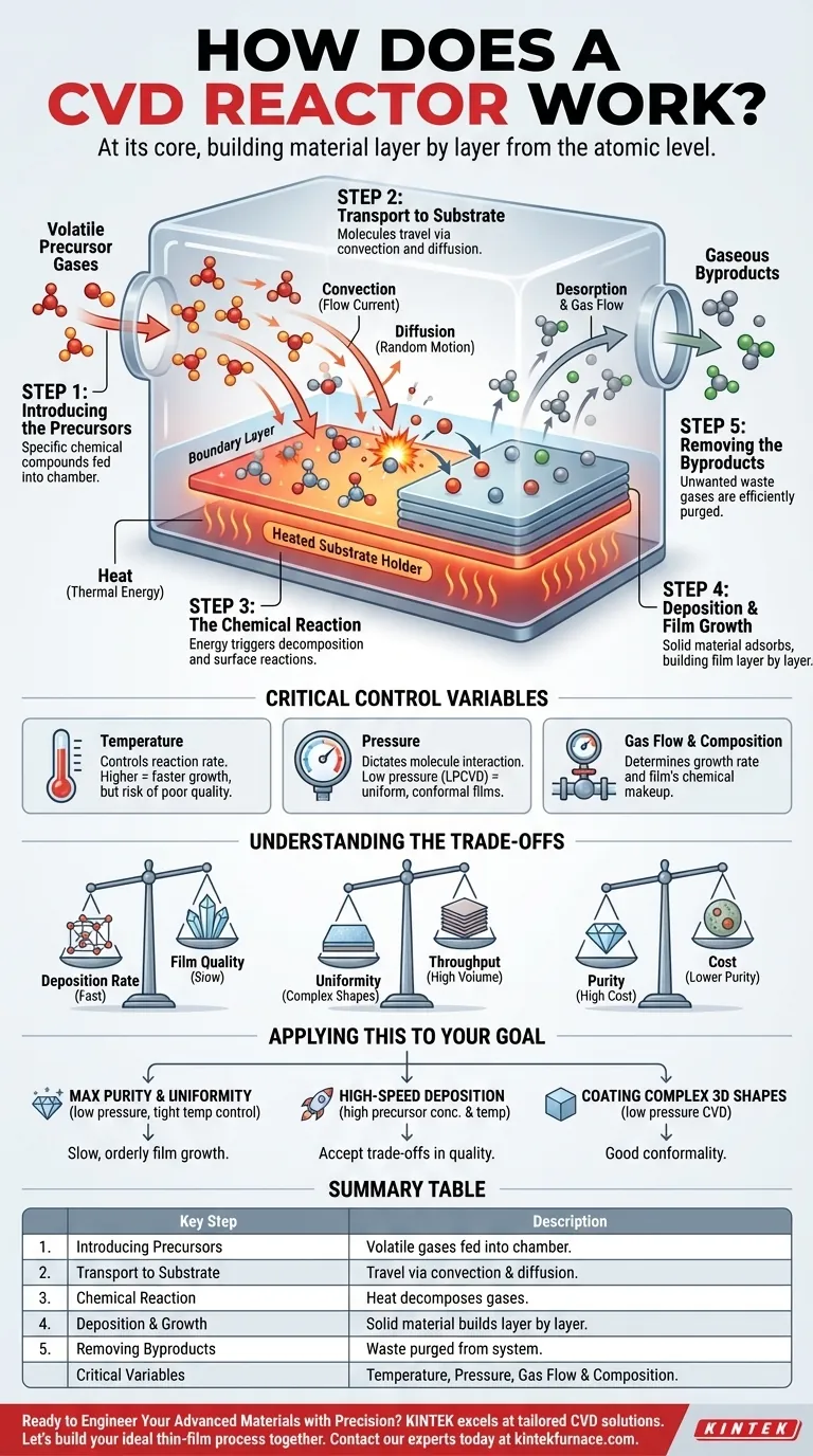
At its core, a Chemical Vapor Deposition (CVD) reactor is a highly controlled environment designed to transform gases into a solid, ultra-thin film on a surface. It works by introducing volatile precursor gases into a chamber containing a substrate. Through a controlled chemical reaction, typically activated by heat, these gases decompose and deposit a solid material, building the desired film layer by layer.
The fundamental principle of CVD is not about carving material away, but about building it up from the atomic level. By precisely managing gas chemistry, temperature, and pressure, a reactor can construct high-purity, uniform films with custom-tailored properties for advanced applications.

The CVD Process: A Step-by-Step Breakdown
To truly understand how a CVD reactor functions, it's best to view it as a sequence of five critical physical and chemical events. Each step must be carefully managed to achieve a high-quality final product.
Step 1: Introducing the Precursors
The process begins by feeding one or more volatile precursor gases into the reaction chamber. These precursors are chemical compounds chosen specifically because they contain the atoms needed for the final film and vaporize at a relatively low temperature.
Step 2: Transport to the Substrate
Once inside the reactor, the precursor molecules travel towards the substrate—the material being coated. This transport happens through two main mechanisms: convection, where the gas flows as a current, and diffusion, the random motion of molecules down a concentration gradient.
As the gas approaches the heated substrate, a thin, slower-moving "boundary layer" forms just above the surface. Precursors must diffuse across this layer to reach the substrate.
Step 3: The Chemical Reaction
This is the heart of the CVD process. The energy supplied to the system, most commonly heat (Thermal CVD), causes the precursor molecules to react and decompose.
These reactions can occur either directly on the hot substrate surface (heterogeneous reaction) or in the gas phase just above it (homogeneous reaction). The goal is to favor surface reactions, which lead to denser, more uniform films.
Step 4: Deposition and Film Growth
The solid product from the chemical reaction adsorbs, or "sticks," to the substrate surface. These atoms then arrange themselves into a stable solid structure, forming a thin film.
The process continues as more precursor molecules arrive, react, and deposit, causing the film to grow in thickness, often one atomic layer at a time.
Step 5: Removing the Byproducts
The chemical reaction almost always produces unwanted gaseous byproducts in addition to the solid film.
These volatile byproducts must be efficiently desorbed from the surface and removed from the chamber by the gas flow. If they are not removed, they can become incorporated into the film as impurities.
The Critical Control Variables
The quality, composition, and thickness of the deposited film are not accidental. They are the direct result of meticulously controlling the reactor's environment.
Temperature
Temperature is the primary knob for controlling the reaction. Higher temperatures increase the reaction rate, leading to faster film growth. However, a temperature that is too high can cause unwanted gas-phase reactions, reducing film quality.
Pressure
The reactor's internal pressure dictates how molecules interact. Low-pressure CVD (LPCVD) increases the distance molecules travel before colliding, which often results in highly uniform films that can coat complex shapes evenly. Atmospheric pressure systems are simpler but can be less uniform.
Gas Flow and Composition
The rate at which precursor gases are introduced and the ratio between them directly determine the film's growth rate and its final chemical makeup. System controls allow for precise management of these gas flows to create films with specific compositions.
Understanding the Trade-offs
CVD is a powerful technique, but it involves balancing competing factors. Understanding these trade-offs is key to successful implementation.
Deposition Rate vs. Film Quality
Generally, faster deposition rates (achieved with higher temperatures or precursor concentrations) can lead to a less-ordered film structure and higher defect counts. Slower, more deliberate growth produces higher-quality, crystalline films.
Uniformity vs. Throughput
Achieving excellent film uniformity, especially over large or complex 3D surfaces, often requires lower pressures and optimized gas flow dynamics. These conditions can slow the overall process, reducing manufacturing throughput.
Purity vs. Cost
The highest-purity films require extremely pure precursor gases and sophisticated reactor designs to prevent contamination. These elements significantly increase the operational cost of the process.
Applying This to Your Goal
Your specific objective dictates how you should approach the CVD process parameters.
- If your primary focus is maximum purity and uniformity: Prioritize a low-pressure process with a tightly controlled temperature to encourage slow, orderly film growth from surface reactions.
- If your primary focus is high-speed deposition: Increase the precursor concentration and temperature, but be prepared to analyze and accept potential trade-offs in film density and structural quality.
- If your primary focus is coating complex 3D shapes: Select a low-pressure CVD method that promotes good conformality, ensuring the precursor gas can diffuse evenly across all surfaces.
Ultimately, the CVD reactor is a masterful tool for engineering materials from the ground up, making it a cornerstone of modern manufacturing in electronics, optics, and beyond.
Summary Table:
| Key CVD Process Step | Description |
|---|---|
| 1. Introducing Precursors | Volatile gases containing the film's atoms are fed into the chamber. |
| 2. Transport to Substrate | Precursors travel via convection and diffusion to the heated surface. |
| 3. Chemical Reaction | Heat decomposes the gases, triggering the deposition reaction. |
| 4. Deposition & Growth | Solid material adsorbs and builds the film layer by layer. |
| 5. Removing Byproducts | Gaseous waste is efficiently desorbed and purged from the system. |
| Critical Control Variables | Temperature, Pressure, Gas Flow & Composition |
Ready to Engineer Your Advanced Materials with Precision?
Whether your goal is maximum film purity, high-speed deposition, or uniform coating of complex 3D structures, the right CVD reactor is critical to your success.
KINTEK excels at delivering tailored CVD solutions that precisely match your unique R&D and production challenges. Leveraging our exceptional in-house R&D and manufacturing capabilities, we provide:
- Advanced CVD & PECVD Systems designed for superior performance and reliability.
- Deep Customization to meet your specific process parameters, substrate materials, and throughput requirements.
- Expert Support to ensure optimal system integration and process development.
Let's build your ideal thin-film process together. Contact our experts today to discuss how a KINTEK CVD reactor can accelerate your innovation.
Visual Guide
Related Products
- MPCVD Machine System Reactor Bell-jar Resonator for Lab and Diamond Growth
- Custom Made Versatile CVD Tube Furnace Chemical Vapor Deposition CVD Equipment Machine
- 915MHz MPCVD Diamond Machine Microwave Plasma Chemical Vapor Deposition System Reactor
- Cylindrical Resonator MPCVD Machine System for Lab Diamond Growth
- Slide PECVD Tube Furnace with Liquid Gasifier PECVD Machine
People Also Ask
- How can the growth rate of diamond be accelerated in the MPCVD method? Boost Growth with Higher Power & Pressure
- What are future trends in MPCVD technology? Unlock Next-Gen Materials with AI and Efficiency
- Why is temperature control important in the MPCVD growth process? Ensure High-Quality, Reliable Diamond Film Deposition
- How does pressure affect the MPCVD growth process? Master Plasma Control for Superior Film Quality
- What are the advantages of MPCVD over LPCVD and PECVD? Achieve Superior Film Quality and Uniformity