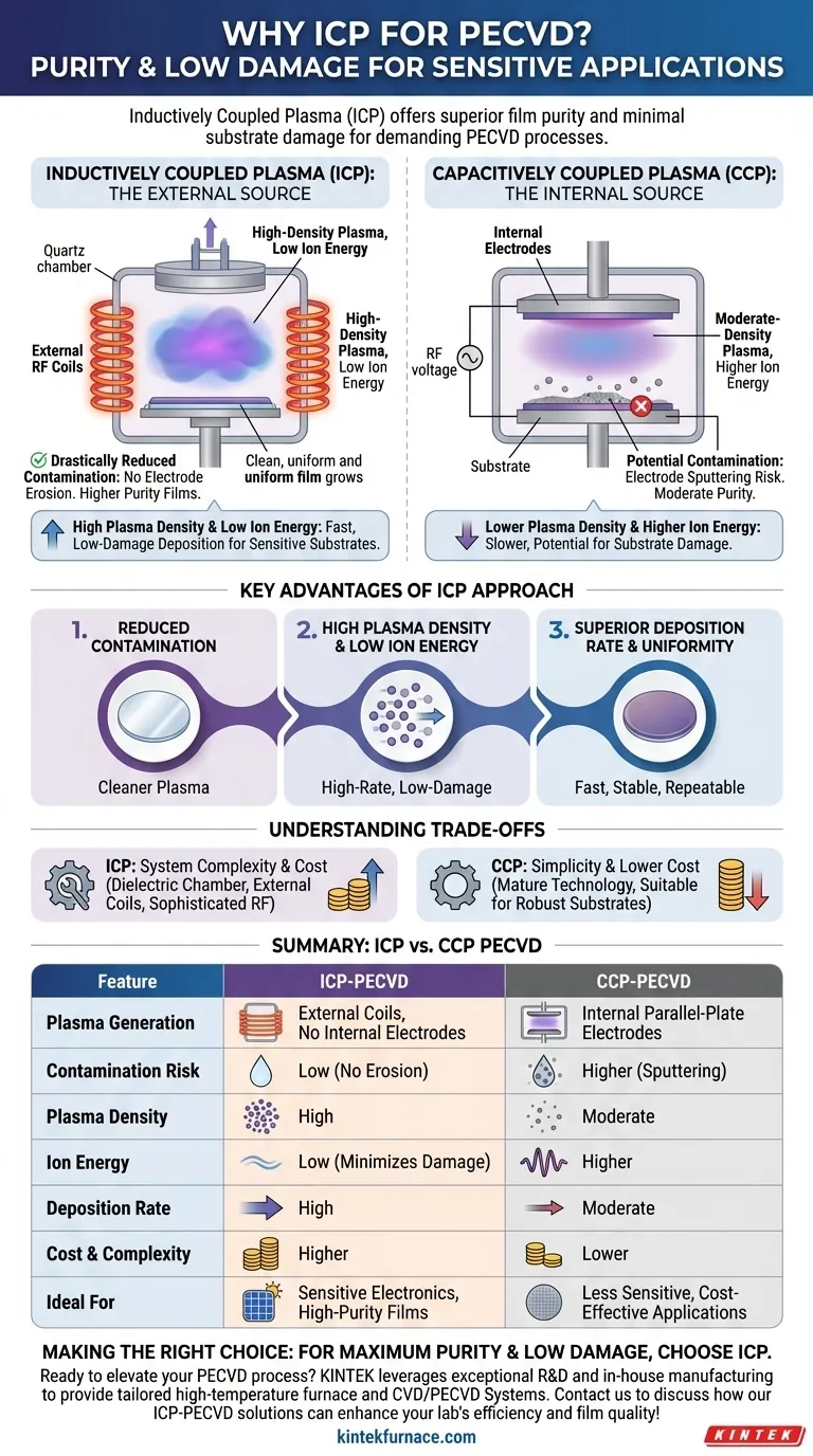
At its core, inductively coupled plasma (ICP) is often preferred for Plasma-Enhanced Chemical Vapor Deposition (PECVD) in applications that demand exceptional film purity and minimal substrate damage. This preference stems from its unique design where the plasma is generated by external coils, preventing the electrode erosion and contamination that can occur in other plasma source designs.
The fundamental choice between plasma sources in PECVD is not about which is universally "better," but about matching the source's characteristics to the specific demands of the application. ICP excels by generating a high-density, low-energy plasma that is physically separate from the hardware, making it ideal for high-rate, low-damage deposition of pure thin films.
The Fundamental Difference: How the Plasma is Generated
The primary distinction between an ICP source and its main alternative, capacitively coupled plasma (CCP), lies in the placement of the electrodes. This single design choice has profound implications for the entire deposition process.
Inductively Coupled Plasma (ICP): The External Source
In an ICP system, radio-frequency (RF) power is applied to antenna coils that are wrapped around the outside of a dielectric chamber wall (e.g., quartz).
This creates a time-varying magnetic field, which in turn induces an electric field inside the chamber. This induced electric field energizes the gas, ionizing it to create a high-density plasma without any internal hardware.
Capacitively Coupled Plasma (CCP): The Internal Source
In contrast, a CCP system uses a parallel-plate capacitor design. The two electrodes are placed directly inside the reaction chamber.
The substrate often sits on the bottom electrode, and an RF voltage applied between the plates ignites and sustains the plasma in the space between them. The electrodes are in direct contact with the reactive plasma they create.
Key Advantages of the ICP Approach
The external nature of the ICP source directly leads to several key performance benefits, making it the superior choice for manufacturing sensitive electronic and optical devices.
Drastically Reduced Contamination
Because the ICP coils are outside the chamber, they are not exposed to the reactive plasma. This eliminates the problem of electrode sputtering or erosion, where atoms from the electrode are knocked off and incorporated into the growing film as impurities.
This results in significantly cleaner plasma and higher-purity films, a critical requirement for high-performance electronics.
High Plasma Density with Low Ion Energy
ICP sources are exceptionally efficient at creating a high density of electrons and reactive species (radicals and ions). This high concentration of precursors accelerates the chemical reactions, enabling very high deposition rates.
Crucially, ICP can achieve this high density at low ion bombardment energies. This means the growing film is not being damaged by high-energy particle bombardment, which is vital for depositing layers on sensitive substrates like those used in solar cells or flexible electronics.
Superior Deposition Rate and Uniformity
The combination of high plasma density and reduced contamination allows for fast, stable, and repeatable film growth. ICP sources can sustain this performance over large areas, making them ideal for high-throughput mass production.
Understanding the Trade-offs
While ICP offers significant advantages, it is not the default choice for every PECVD process. Understanding its trade-offs is key to making an informed decision.
System Complexity and Cost
ICP-PECVD reactors are generally more mechanically complex and expensive than their CCP counterparts. The design requires a dielectric chamber, external RF coils, and often more sophisticated RF matching networks to efficiently couple power into the plasma.
When CCP Is the Right Choice
For many applications where ultimate film purity is not the primary concern and the substrate is robust, the simplicity and lower cost of a CCP system make it a more practical choice. CCP is a mature, reliable technology that is perfectly suitable for a wide range of standard thin-film applications.
Making the Right Choice for Your Application
The decision to use ICP or another plasma source must be driven by the end goal of your deposition process.
- If your primary focus is maximum film purity and low substrate damage: Choose ICP. It is the superior technology for manufacturing high-efficiency solar cells, advanced transistors, and other sensitive semiconductor devices.
- If your primary focus is cost-effectiveness for less-sensitive applications: CCP is often the more practical and economical choice, offering reliable performance for a wide range of materials where minor impurities or higher ion energy are acceptable.
Ultimately, selecting the right plasma source is a strategic engineering decision that balances the stringent performance requirements of the device against the practical constraints of system cost and complexity.
Summary Table:
| Feature | ICP-PECVD | CCP-PECVD |
|---|---|---|
| Plasma Generation | External coils, no internal electrodes | Internal parallel-plate electrodes |
| Contamination Risk | Low (no electrode erosion) | Higher (electrode sputtering possible) |
| Plasma Density | High | Moderate |
| Ion Energy | Low (minimizes substrate damage) | Higher |
| Deposition Rate | High | Moderate |
| Cost & Complexity | Higher | Lower |
| Ideal For | Sensitive electronics, high-purity films | Less sensitive, cost-effective applications |
Ready to elevate your PECVD process with high-purity, low-damage thin films?
At KINTEK, we leverage exceptional R&D and in-house manufacturing to provide advanced high-temperature furnace solutions, including our specialized CVD/PECVD Systems. Our strong deep customization capability ensures we can precisely meet your unique experimental requirements, whether you're working on sensitive semiconductor devices, solar cells, or other demanding applications.
Contact us today to discuss how our tailored ICP-PECVD solutions can enhance your lab's efficiency and film quality!
Visual Guide
Related Products
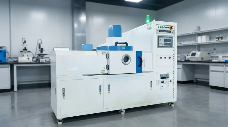
- Inclined Rotary Plasma Enhanced Chemical Deposition PECVD Tube Furnace Machine
- Inclined Rotary Plasma Enhanced Chemical Deposition PECVD Tube Furnace Machine
- Slide PECVD Tube Furnace with Liquid Gasifier PECVD Machine
- RF PECVD System Radio Frequency Plasma Enhanced Chemical Vapor Deposition
- Multi Heating Zones CVD Tube Furnace Machine for Chemical Vapor Deposition Equipment
People Also Ask
- What types of materials can be processed in rotary tube furnaces? Optimize Your Thermal Processing with Versatile Solutions
- What is plasma in the context of PECVD? Unlock Low-Temperature Thin Film Deposition
- What are the main advantages of PECVD tube furnaces compared to CVD tube furnaces? Lower Temp, Faster Deposition, and More
- When are rotary tube furnaces not suitable for a process? Avoid Costly Mistakes in Thermal Processing
- How does the temperature control system work in a rotary tube furnace? Achieve Precise Thermal Processing for Your Materials


