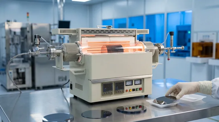
In semiconductor wafer processing, vacuum furnaces are essential for thermal treatments that repair and purify silicon wafers. They provide an ultra-clean, high-temperature environment required for critical manufacturing steps. Key processes like annealing and gettering are performed in these furnaces to reduce crystalline defects and remove atomic-level impurities, directly improving the electrical performance and reliability of the final microchips.
The core challenge in semiconductor fabrication is achieving near-perfect purity and structural integrity in the silicon crystal. A vacuum furnace solves this by removing atmospheric gases—especially oxygen—that would otherwise contaminate the wafer and create performance-killing defects at the high temperatures required for processing.
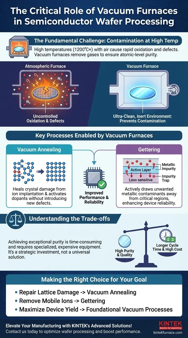
The Fundamental Problem: Contamination at High Temperatures
To understand the role of a vacuum furnace, you must first understand the primary enemy in semiconductor manufacturing: unwanted contamination.
Why a Vacuum is Non-Negotiable
A standard industrial furnace heats materials in the presence of air, which is composed of nitrogen, oxygen, and other trace gases.
At the high temperatures used in wafer processing, typically above 1200°C, oxygen becomes highly reactive. It will aggressively bond with the silicon wafer, a process called oxidation.
While some controlled oxidation is necessary, uncontrolled oxidation creates defects and contaminates the silicon. A vacuum furnace prevents this by using pumps to remove the air from its chamber, creating an airtight, controlled environment free from reactive gases.
The Goal: Atomic-Level Purity
Semiconductor devices function by precisely controlling the flow of electrons through a near-perfect silicon crystal lattice.
This control is achieved by intentionally introducing tiny, specific amounts of impurities, known as dopants. Any other unintentional impurity or structural defect in the crystal can disrupt this electron flow, causing device failure.
A vacuum furnace provides the pristine environment necessary to perform thermal treatments without introducing these unwanted contaminants, ensuring the wafer's purity and structural integrity are maintained.
Key Processes Enabled by Vacuum Furnaces
The clean, controlled environment of a vacuum furnace is not just a passive safeguard; it actively enables critical restorative and purification processes.
Vacuum Annealing: Healing the Crystal Structure
Manufacturing steps like ion implantation, where dopants are fired into the wafer, cause significant damage to the silicon's crystal lattice.
Vacuum annealing is a process where the wafer is heated to high temperatures. This gives the displaced silicon atoms the thermal energy needed to move back into their correct positions, effectively "healing" the crystal structure and electrically activating the dopants.
Performing this step in a vacuum is critical. It ensures that while the crystal is being repaired, no new defects are created through oxidation or contamination.
Gettering: Actively Removing Impurities
Even with extreme care, microscopic metallic impurities (like iron or copper) can find their way onto a wafer. These mobile ions are devastating to device performance.
Gettering is a thermal process that uses the vacuum furnace to draw these unwanted contaminants away from the active, critical regions of the wafer and trap them in a less sensitive area. It functions as a final, high-powered purification step to enhance wafer quality and device yield.
Understanding the Trade-offs
While indispensable, vacuum furnaces are a specific tool with inherent trade-offs that engineers must manage.
Cycle Time vs. Purity
Vacuum furnaces are not fast. Achieving a high vacuum, heating the chamber, holding at temperature, and cooling down is a time-consuming process.
This creates a trade-off between purity and throughput. While the results are exceptionally clean, the cycle time can be a bottleneck in a high-volume manufacturing line compared to faster, atmospheric-based thermal processes.
Cost and Complexity
These are highly specialized and expensive machines. They require significant infrastructure for powerful vacuum pumps, high-purity gas lines, and sophisticated control systems.
The operational and maintenance costs are substantial, representing a major capital investment dedicated to achieving the highest levels of material purity.
Not a Universal Solution
Vacuum furnaces are not used for every thermal step. Certain processes, such as the deliberate growth of a high-quality silicon dioxide layer, intentionally use a furnace filled with pure oxygen.
The choice of furnace—vacuum, atmospheric, or a specific controlled gas environment—is dictated entirely by the precise goal of the manufacturing step.
Making the Right Choice for Your Goal
The use of a vacuum furnace is directly tied to the need for an inert thermal environment that prevents unwanted reactions.
- If your primary focus is repairing lattice damage and activating dopants: You will rely on vacuum annealing to provide a clean, high-temperature environment without introducing new contaminants.
- If your primary focus is removing mobile metallic ions: You will use a gettering process within a vacuum furnace to draw these impurities away from the critical device layers, boosting reliability.
- If your primary focus is ensuring maximum device yield and performance: Using a vacuum furnace for key steps is foundational, as it directly minimizes the oxide and metallic contamination that leads to device failure.
Ultimately, mastering the vacuum furnace environment is a prerequisite for producing the high-performance, reliable semiconductor devices that power modern electronics.
Summary Table:
| Process | Purpose | Key Benefit |
|---|---|---|
| Vacuum Annealing | Heals crystal damage from ion implantation | Activates dopants and repairs silicon lattice without contamination |
| Gettering | Removes metallic impurities | Enhances device yield and reliability by purifying wafers |
| General Use | Provides ultra-clean, high-temperature environment | Prevents oxidation and contamination for superior electrical performance |
Elevate your semiconductor manufacturing with KINTEK's advanced vacuum furnace solutions! Leveraging exceptional R&D and in-house manufacturing, we offer a diverse product line including Vacuum & Atmosphere Furnaces and CVD/PECVD Systems, tailored for precise thermal treatments. Our strong deep customization capability ensures we meet your unique experimental needs, delivering high purity and reliability. Contact us today to discuss how our solutions can optimize your wafer processing and boost device performance!
Visual Guide
Related Products
- Vacuum Hot Press Furnace Machine Heated Vacuum Press Tube Furnace
- Vacuum Hot Press Furnace Machine Heated Vacuum Press
- 600T Vacuum Induction Hot Press Vacuum Heat Treat and Sintering Furnace
- 2200 ℃ Tungsten Vacuum Heat Treat and Sintering Furnace
- Vacuum Heat Treat Sintering Furnace with Pressure for Vacuum Sintering
People Also Ask
- What is the primary function of the vacuum environment in a vacuum hot press furnace during titanium alloy processing? Prevent Embrittlement for Superior Ductility
- What considerations guide the selection of heating elements and pressurization methods for a vacuum hot press furnace?
- What safety features are incorporated in vacuum hot press furnaces? Ensure Operator and Equipment Protection
- How have vacuum hot press furnaces transformed material processing? Achieve Superior Density and Purity
- What temperature control features do vacuum hot press furnaces have? Achieve Precision in High-Temp Material Processing


