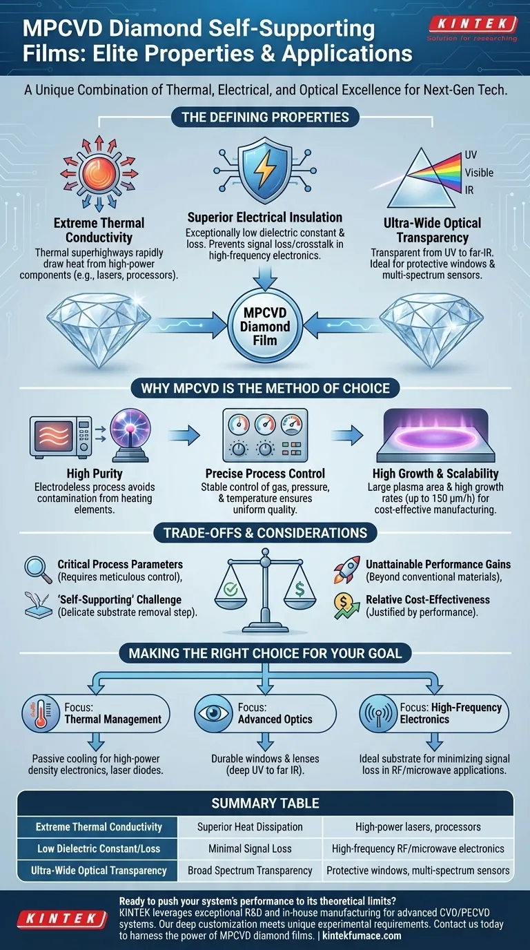
In short, diamond self-supporting films prepared using Microwave Plasma Chemical Vapor Deposition (MPCVD) are defined by a unique combination of three elite properties. They possess extremely high thermal conductivity for heat management, exceptionally low dielectric constant and loss for high-frequency electronics, and ultra-wide optical transparency for advanced optical systems.
These films represent the successful translation of diamond's theoretical material advantages into a practical, high-purity form. The MPCVD process is what makes it possible to create these films with the consistency and quality required for demanding next-generation applications.
The Defining Properties of MPCVD Diamond Films
The unique value of these films comes from combining properties that are rarely found together in a single material.
Extreme Thermal Conductivity
Diamond is the most thermally conductive material known at room temperature. MPCVD-grown films harness this property, acting as "thermal superhighways" that can rapidly draw heat away from critical components like high-power lasers or advanced processors.
Superior Electrical Insulation
These films have a very low dielectric constant and dielectric loss. This makes them exceptional electrical insulators, especially for high-frequency signals. They prevent signal loss and crosstalk in advanced RF and microwave electronics, enabling more powerful and efficient devices.
Ultra-Wide Optical Transparency
MPCVD diamond is transparent across an exceptionally broad range of the electromagnetic spectrum, from ultraviolet (UV) to far-infrared (IR) and microwaves. This makes it an ideal material for protective windows and lenses in harsh environments or for multi-spectrum sensor applications.
Why MPCVD is the Method of Choice
Not all diamond synthesis methods are equal. MPCVD offers specific advantages that are critical for producing the high-quality, free-standing films required for technical applications.
High Purity and Contamination Avoidance
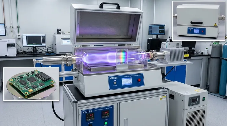
Unlike older "hot filament" methods, MPCVD uses microwaves to generate plasma. This electrodeless process avoids contamination from heating elements, resulting in a diamond film of significantly higher purity and quality.
Precise and Stable Process Control
The quality of the final diamond film depends entirely on a precise recipe. MPCVD allows for stable, accurate control over the critical parameters: the gas mixture, chamber pressure, and substrate temperature. This ensures reproducible quality and uniform thickness.
High Growth Rates and Scalability
MPCVD technology facilitates a large and stable plasma area, enabling uniform deposition over larger surfaces. Combined with high growth rates (up to 150 μm/h), this makes the process more scalable and cost-effective for manufacturing compared to other high-purity diamond synthesis techniques.
Understanding the Trade-offs and Considerations
While the properties are outstanding, it is crucial to understand the context and challenges associated with producing these films.
The Criticality of Process Parameters
The exceptional quality of MPCVD diamond is not automatic. It is the direct result of meticulous control over the deposition process. Any deviation in temperature, pressure, or gas composition can degrade the film's properties, introducing impurities or internal stress.
Cost-Effectiveness is Relative
While MPCVD is considered cost-effective compared to other specialized CVD diamond techniques, it remains a highly sophisticated and capital-intensive process. The cost is justified by performance gains that are unattainable with conventional materials like silicon or glass.
The "Self-Supporting" Challenge
Creating a "self-supporting" film means it must first be grown on a substrate (like silicon) and then separated from it. This removal process is a delicate and critical manufacturing step that can impact yield, cost, and the final integrity of the film.
Making the Right Choice for Your Goal
To determine if MPCVD diamond is the correct material, align its primary benefits with your specific technical goal.
- If your primary focus is thermal management: MPCVD diamond is an unparalleled choice for passive cooling of high-power density electronics, laser diodes, or GaN devices.
- If your primary focus is advanced optics: Use these films for durable windows and lenses that require transparency across multiple spectrums, from deep UV to far IR.
- If your primary focus is high-frequency electronics: MPCVD diamond serves as an ideal substrate material to minimize signal loss and improve performance in RF, microwave, and millimeter-wave applications.
Ultimately, leveraging MPCVD diamond films allows you to engineer systems that operate closer to their theoretical limits.
Summary Table:
| Property | Key Benefit | Application Example |
|---|---|---|
| Extreme Thermal Conductivity | Superior heat dissipation | High-power lasers, processors |
| Low Dielectric Constant/Loss | Minimal signal loss | High-frequency RF/microwave electronics |
| Ultra-Wide Optical Transparency | Broad spectrum transparency (UV to far-IR) | Protective windows, multi-spectrum sensors |
Ready to push your system's performance to its theoretical limits?
At KINTEK, we leverage our exceptional R&D and in-house manufacturing to provide diverse laboratories with advanced high-temperature furnace solutions, including our specialized CVD/PECVD systems. Our expertise is crucial for producing the high-purity, self-supporting diamond films discussed here.
Whether your project requires unparalleled thermal management, advanced optics, or high-frequency electronics, our strong deep customization capability allows us to precisely meet your unique experimental requirements for MPCVD processes.
Contact us today to discuss how our tailored solutions can help you harness the power of MPCVD diamond films for your next-generation application.
Visual Guide
Related Products
- 915MHz MPCVD Diamond Machine Microwave Plasma Chemical Vapor Deposition System Reactor
- MPCVD Machine System Reactor Bell-jar Resonator for Lab and Diamond Growth
- Cylindrical Resonator MPCVD Machine System for Lab Diamond Growth
- HFCVD Machine System Equipment for Drawing Die Nano Diamond Coating
- Multi Heating Zones CVD Tube Furnace Machine for Chemical Vapor Deposition Equipment
People Also Ask
- What are the essential components of an MPCVD reactor for diamond film deposition? Unlock High-Quality Diamond Growth
- What are some key features and benefits of the microwave plasma chemical vapor deposition system? Achieve Unmatched Material Synthesis
- What factors influence the quality of diamond deposition in the MPCVD method? Master the Critical Parameters for High-Quality Diamond Growth
- How does the MPCVD process work to deposit diamond? A Guide to High-Purity Synthesis
- In which industries is the microwave plasma chemical vapor deposition system commonly used? Unlock High-Purity Material Synthesis


