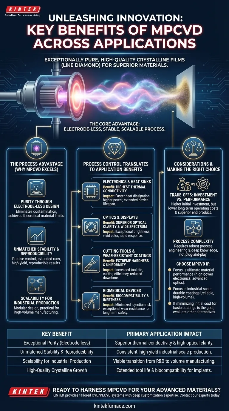
The fundamental benefit of MPCVD is its ability to grow exceptionally pure, high-quality crystalline films, most notably diamond, with a level of control and consistency that other methods struggle to match. This precision enables the creation of materials with superior physical properties, unlocking significant performance gains across a wide range of advanced industrial applications, from semiconductors to biomedical devices.
The core advantage of Microwave Plasma Chemical Vapor Deposition (MPCVD) lies not just in the superior end-product, but in the process itself. Its electrode-less, stable, and scalable nature is what makes the production of high-purity, high-performance materials a repeatable and industrially viable reality.
The Process Advantage: Why MPCVD Excels
The specific benefits seen in final products originate from the inherent advantages of the MPCVD manufacturing process itself. It is engineered to overcome the common limitations of other deposition techniques.
Purity Through an Electrode-less Design
Unlike other methods that use hot filaments or electrodes inside the reaction chamber, MPCVD uses microwaves to generate plasma. This electrode-less process is critical, as it eliminates a major source of contamination.
The result is a film of exceptional purity, which is directly responsible for achieving the theoretical limits of the material's properties, such as thermal conductivity or optical clarity.
Unmatched Stability and Reproducibility
MPCVD systems create a large, stable plasma area and allow for precise, stable control over temperature and gas composition.
This stability means the process can run continuously for extended periods without degrading the quality of the film. For industrial applications, this translates to high-yield, reproducible results from one batch to the next.
Scalability for Industrial Production
The technology is built on a modular and scalable design. Systems can be adapted to accommodate larger substrates or linked together for high-volume manufacturing.
This inherent scalability makes MPCVD a practical choice for moving from laboratory-scale research to full industrial production, ensuring the economic viability of the final product.
How Process Control Translates to Application Benefits
The purity, quality, and consistency enabled by the MPCVD process are the direct causes of the performance breakthroughs seen in various fields.
For Electronics and Heat Sinks
The near-perfect crystal structure achieved with MPCVD results in diamond films with the highest possible thermal conductivity.
For semiconductors, this means faster and more efficient heat dissipation, allowing devices to run at higher power levels without overheating. This directly improves performance and extends the lifespan of electronic components.
For Optics and Displays
The lack of impurities and defects yields diamond with superior optical clarity and a very wide transmittance spectrum, from UV to infrared.
In applications like high-resolution displays or specialized optical windows, this translates to exceptional brightness, vivid color, and rapid response times, which are vital for detailed imaging systems.
For Cutting Tools and Wear-Resistant Coatings
MPCVD can deposit a uniform, incredibly hard diamond film onto cutting tools and other industrial parts. This layer’s extreme hardness and low friction are a direct result of the high-quality crystal growth.
This leads to a dramatic increase in tool life and cutting efficiency. It also reduces manufacturing costs by minimizing downtime and the need for frequent tool replacement.
For Biomedical Devices
The inert and pure carbon structure of MPCVD diamond makes it highly biocompatible. The body does not recognize it as a foreign material, minimizing the risk of rejection.
When used as a coating on implants or surgical tools, its hardness also provides exceptional wear resistance, ensuring the long-term integrity and safety of the device.
Understanding the Trade-offs and Considerations
While powerful, MPCVD is a sophisticated technology, and its adoption requires a clear understanding of the balance between investment and performance.
Initial Investment vs. Long-Term Value
MPCVD systems represent a significant capital investment compared to simpler methods like Hot Filament CVD (HFCVD). The equipment involves precise microwave generators, vacuum systems, and cooling.
However, for applications where maximum performance, purity, and reliability are non-negotiable, the higher initial cost is often justified by lower operating costs, reduced downtime, and the superior quality of the end product. It is often more cost-effective than other high-end CVD techniques for the quality it delivers.
Process Complexity
Achieving optimal results with MPCVD requires deep process knowledge and control over multiple variables, including gas mixture, pressure, temperature, and microwave power.
This complexity means that successful implementation depends on robust process engineering. It is not a "plug-and-play" solution but a highly controlled industrial process for creating high-value materials.
Making the Right Choice for Your Goal
Your application's specific requirements will determine if MPCVD is the most effective technology for you.
- If your primary focus is ultimate material performance: For demanding applications in high-power electronics, advanced optics, or medical implants where purity and crystal quality are paramount, MPCVD is the industry-leading choice.
- If your primary focus is industrial-scale production of durable coatings: MPCVD’s unique combination of high growth rates, stability, and scalability makes it ideal for manufacturing reliable, high-performance tools and components at volume.
- If your primary focus is minimizing initial capital cost for basic coatings: For less demanding applications where some level of impurity is acceptable, you should evaluate MPCVD against simpler, lower-cost deposition alternatives.
Ultimately, MPCVD empowers engineers and scientists to move beyond the limitations of conventional materials by providing a reliable pathway to manufacturing near-perfect crystalline films.
Summary Table:
| Key Benefit | Primary Application Impact |
|---|---|
| Exceptional Purity (Electrode-less Design) | Superior thermal conductivity for electronics; high optical clarity for displays and lenses. |
| Unmatched Stability & Reproducibility | Consistent, high-yield production for industrial-scale manufacturing. |
| Scalability for Industrial Production | Viable transition from R&D to volume manufacturing of coatings and components. |
| High-Quality Crystalline Growth | Extended tool life for cutting applications; biocompatibility for medical implants. |
Ready to harness the power of MPCVD for your advanced materials? At KINTEK, we leverage our exceptional R&D and in-house manufacturing capabilities to provide tailored high-temperature furnace solutions, including advanced CVD/PECVD systems. Our strong deep customization expertise ensures we can meet your unique experimental and production requirements for growing high-purity diamond films. Contact our experts today to discuss how our MPCVD technology can drive your innovation forward!
Visual Guide
Related Products
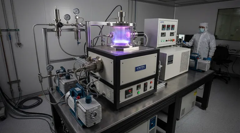
- 915MHz MPCVD Diamond Machine Microwave Plasma Chemical Vapor Deposition System Reactor
- MPCVD Machine System Reactor Bell-jar Resonator for Lab and Diamond Growth
- Cylindrical Resonator MPCVD Machine System for Lab Diamond Growth
- Multi Heating Zones CVD Tube Furnace Machine for Chemical Vapor Deposition Equipment
- Inclined Rotary Plasma Enhanced Chemical Deposition PECVD Tube Furnace Machine
People Also Ask
- What factors influence the quality of diamond deposition in the MPCVD method? Master the Critical Parameters for High-Quality Diamond Growth
- What is the purpose of a microwave plasma chemical vapor deposition system? Grow High-Purity Diamonds and Advanced Materials
- What is the basic principle of operation for the microwave plasma chemical vapor deposition system? Unlock High-Purity Material Growth
- What are the essential components of an MPCVD reactor system? Build a Pristine Environment for High-Purity Materials
- In which industries is the microwave plasma chemical vapor deposition system commonly used? Unlock High-Purity Material Synthesis


