At its core, Chemical Vapor Deposition (CVD) is a cornerstone manufacturing process used to create high-performance thin films and coatings. Its applications are remarkably diverse, spanning from the production of microchips in the semiconductor industry to creating protective layers on jet engine turbines and biocompatible coatings for medical implants.
The true value of CVD isn't just its wide range of applications, but why it is so versatile. Its power comes from its unique ability to build materials atom-by-atom from a gas phase, enabling the creation of exceptionally pure, uniform, and conformal coatings on almost any surface, regardless of its shape.
The Foundation of Modern Electronics
CVD is not merely a tool in the semiconductor industry; it is the fundamental process that makes modern electronics possible. The ability to deposit pristine, ultra-thin layers of different materials is the basis for creating complex micro-architectures.
Building Integrated Circuits (ICs)
The transistors and wires that make up a computer chip are built from stacked layers of materials. CVD is the primary method used to deposit these critical layers, including insulating films like silicon nitride, conductive metal layers, and the semiconducting films that form the heart of the transistor.
Powering Photovoltaics and Optical Devices
CVD is essential for producing the thin films in photovoltaic devices (solar cells) that convert sunlight into electricity. In the optics industry, it's used to apply anti-reflective coatings on lenses and create other specialized optical filters with high precision.
Engineering for Extreme Environments
Many industries rely on components that must perform flawlessly under intense heat, pressure, and chemical exposure. CVD provides a way to fortify these components with engineered surfaces.
Protecting Aerospace Components
CVD is used to apply thermal barrier coatings to aerospace parts, such as turbine blades in jet engines. These ceramic coatings protect the underlying metal from extreme temperatures, significantly extending the component's lifespan and reliability.
Creating Wear-Resistant Surfaces
For industrial tools, bearings, and other parts subject to friction and wear, CVD can deposit extremely hard ceramic coatings. These layers dramatically improve durability and reduce the need for maintenance.
Advancing Human Health and Materials Science
The precision of CVD allows it to operate at the intersection of material science and biology, creating surfaces with specialized functions.
Enhancing Biocompatibility
Medical implants, from artificial joints to dental implants, must be accepted by the body without causing an adverse reaction. CVD is used to apply inert, biocompatible coatings that enhance integration and reduce the risk of rejection.
Innovating Drug Delivery
The process can be used to create highly specific coatings and structures for advanced drug delivery systems. These systems can be designed to release medication more efficiently or target specific cells within the body.
Synthesizing Advanced Materials
CVD is a key method for synthesizing next-generation materials like graphene and carbon nanotubes. These materials possess extraordinary electrical, thermal, and mechanical properties, and CVD provides the control needed to grow them for research and commercial applications.
Understanding the Core Advantages
The widespread adoption of CVD is a direct result of several key technical advantages that other deposition methods often cannot match.
Advantage: Unmatched Purity and Control
Because the precursor materials are introduced as high-purity gases, CVD can produce films with exceptional purity, often exceeding 99.995%. This is non-negotiable for semiconductor manufacturing, where even minuscule impurities can ruin a device.
Advantage: Conformal Coating on Any Shape
Reactant gases naturally flow around and into every feature of a substrate. This allows CVD to deposit a perfectly uniform, or conformal, film over complex, three-dimensional, and irregularly shaped surfaces—a critical capability for microelectronics and intricate mechanical parts.
Advantage: Material Versatility
CVD is not limited to one class of material. The process can be adapted to deposit a vast range of materials, including metals, alloys, ceramics (like nitrides and oxides), and even polymers.
The Caveat: Process Conditions
The primary trade-off with CVD is its operational requirements. Many CVD processes require high temperatures and involve precursor gases that can be hazardous or expensive. Managing these conditions is a key engineering challenge but is necessary to achieve the high-quality results the method is known for.
Making the Right Choice for Your Goal
Deciding if CVD is the appropriate method depends entirely on your primary material and performance requirements.
- If your primary focus is electronic performance: CVD is the industry standard for creating the ultra-pure, defect-free thin films required for semiconductors.
- If your primary focus is durability in harsh environments: CVD provides robust ceramic and metallic coatings ideal for protecting components in aerospace and industrial applications.
- If your primary focus is biocompatibility: CVD is an excellent choice for modifying the surface of medical implants to ensure they are safely accepted by the body.
- If your primary focus is coating complex shapes uniformly: CVD's gas-phase nature makes it superior to many line-of-sight methods for creating conformal layers on intricate geometries.
Ultimately, CVD is the definitive process when the performance and reliability of your final product are determined by the quality and precision of its surface.
Summary Table:
| Application Area | Key CVD Uses |
|---|---|
| Electronics & Semiconductors | Building integrated circuits (ICs), transistors, and photovoltaic films. |
| Extreme Environments | Thermal barrier coatings for aerospace, wear-resistant surfaces for industrial tools. |
| Medical & Biotechnology | Biocompatible coatings for implants, advanced drug delivery systems. |
| Advanced Materials | Synthesizing graphene, carbon nanotubes, and other next-generation materials. |
| Core Advantages | Unmatched purity, conformal coating on complex shapes, material versatility. |
Ready to leverage the precision of CVD for your advanced manufacturing or R&D goals?
At KINTEK, we understand that achieving exceptional thin film results requires more than just a standard furnace. Our expertise lies in providing advanced high-temperature furnace solutions, including our specialized CVD/PECVD Systems, which are engineered to meet the demanding process conditions of Chemical Vapor Deposition.
Leveraging exceptional R&D and in-house manufacturing, we offer:
- Tailored CVD Solutions: Our strong deep customization capability allows us to precisely configure systems to your unique material, substrate, and performance requirements.
- Proven Performance: From semiconductor research to coating complex industrial components, our furnaces deliver the purity, uniformity, and control that CVD demands.
Let's discuss how a KINTEK CVD system can become the cornerstone of your next innovation. Contact our experts today for a consultation to explore the perfect solution for your application.
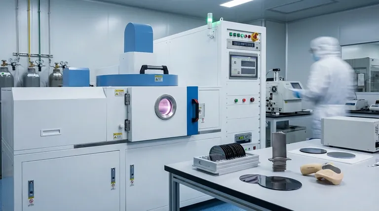
Visual Guide
Related Products
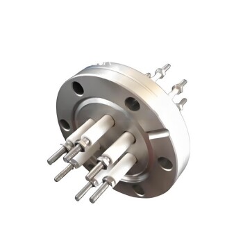
- Custom Made Versatile CVD Tube Furnace Chemical Vapor Deposition CVD Equipment Machine
- Multi Heating Zones CVD Tube Furnace Machine for Chemical Vapor Deposition Equipment
- HFCVD Machine System Equipment for Drawing Die Nano Diamond Coating
- Split Chamber CVD Tube Furnace with Vacuum Station CVD Machine
- 915MHz MPCVD Diamond Machine Microwave Plasma Chemical Vapor Deposition System Reactor
People Also Ask
- How does CVD tube furnace sintering enhance graphene growth? Achieve Superior Crystallinity and High Electron Mobility
- How can integrating CVD tube furnaces with other technologies benefit device fabrication? Unlock Advanced Hybrid Processes
- What is the working principle of a CVD tube furnace? Achieve Precise Thin Film Deposition for Your Lab
- What are the key features of CVD tube furnaces for 2D material processing? Unlock Precision Synthesis for Superior Materials
- What future trends are expected in the development of CVD tube furnaces? Discover Smarter, More Versatile Systems