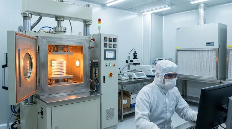
In modern electronics, a Vacuum Hot Press is not just a tool but an enabling technology. It is used to produce high-density ceramic substrates for microchips, to bond and sinter multi-material semiconductor wafers, and to fabricate critical thermal management components like heat spreaders that prevent devices from overheating. These processes are all performed under a controlled vacuum to ensure the highest possible material purity and structural integrity.
The core function of a Vacuum Hot Press is to solve the fundamental material science challenges of modern electronics. By applying heat and pressure in a vacuum, it eliminates the contamination, oxidation, and microscopic voids that would otherwise cripple the performance and reliability of high-performance semiconductor components.
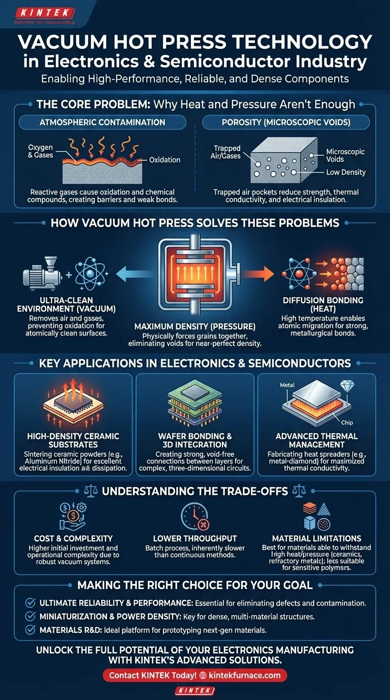
The Core Problem: Why Heat and Pressure Aren't Enough
To understand the role of vacuum hot pressing, you must first understand the limitations of processing materials in a normal atmosphere. Applying heat and pressure alone is insufficient for the demands of advanced electronics.
The Challenge of Atmospheric Contamination
At the high temperatures required for sintering and bonding, materials become highly reactive. Any oxygen or other atmospheric gases present will immediately cause oxidation and form unwanted chemical compounds on the material's surface.
These contaminant layers act as barriers, preventing a true, strong bond from forming between particles or layers. This results in weak, unreliable components with poor electrical and thermal performance.
The Problem of Porosity
When powders are pressed into a solid part (sintering), tiny pockets of air can become trapped between the grains. These microscopic voids, known as porosity, degrade almost every important property of the material.
Porosity reduces mechanical strength, hinders thermal conductivity by disrupting the path for heat to escape, and can compromise the electrical insulation properties of a substrate.
How the Vacuum Hot Press Solves These Problems
The Vacuum Hot Press systematically eliminates these issues by creating a precisely controlled environment. It combines three critical elements: high temperature, mechanical pressure, and a high-vacuum atmosphere.
It Creates an Ultra-Clean Environment
The vacuum is the most critical element. By removing the air and other reactive gases, it prevents oxidation and contamination. This ensures that the surfaces being joined are atomically clean, which is a prerequisite for the strongest possible bond.
It Achieves Maximum Density
Simultaneous pressure physically forces the material grains together, collapsing the microscopic voids that would otherwise become trapped porosity. The vacuum helps pull any remaining trapped gases out of the structure.
The result is a component with near-perfect density, maximizing its strength, thermal conductivity, and overall performance.
It Enables Diffusion Bonding
With clean surfaces and no voids, the applied heat and pressure enable diffusion bonding. This is a solid-state process where atoms from one material surface migrate across the boundary to interlock with the atoms of the other.
This creates a bond that is not just mechanical but metallurgical, resulting in a single, seamless component with no weak interface.
Key Applications in Electronics & Semiconductors
The unique capabilities of vacuum hot pressing directly translate to the manufacturing of mission-critical electronic components.
High-Density Ceramic Substrates
Microchips are built on substrates that must provide excellent electrical insulation while also efficiently dissipating heat. A Vacuum Hot Press is used to sinter ceramic powders (like Aluminum Nitride) into fully dense substrates, free from the voids that would compromise these properties.
Wafer Bonding and 3D Integration
Modern chip design involves stacking multiple layers of different semiconductor materials. Vacuum hot pressing is used for wafer bonding, creating strong, void-free connections between these layers to build complex, three-dimensional integrated circuits.
Advanced Thermal Management
High-power electronics generate immense heat that must be removed. A Vacuum Hot Press fabricates advanced heat spreaders from materials like metal-diamond composites. The process ensures there are no voids at the metal-diamond interface, guaranteeing the highest possible thermal conductivity to protect the chip.
Understanding the Trade-offs
While powerful, this technology is not a universal solution. It involves specific trade-offs that make it suitable for high-value applications.
Cost and Complexity
Vacuum Hot Press systems are significantly more expensive and complex to operate than atmospheric furnaces. The need for robust vacuum chambers, pumps, and precise controls adds to the initial investment and operational overhead.
Lower Throughput
The process of creating a vacuum, running the heating and pressing cycle, and cooling down is inherently time-consuming. This makes vacuum hot pressing a batch process, which is slower than continuous atmospheric methods.
Material Limitations
The process is best suited for materials that can withstand high temperatures and pressures without degrading. This includes ceramics, refractory metals, and certain composites, but it may not be suitable for more sensitive polymers or low-melting-point alloys.
Making the Right Choice for Your Goal
Selecting this process depends entirely on the required level of performance and reliability for the final component.
- If your primary focus is ultimate reliability and performance: A Vacuum Hot Press is essential to eliminate the microscopic defects and contamination that cause component failure.
- If your primary focus is miniaturization and power density: This technology is the key to creating the dense, multi-material structures required for advanced 3D packaging and efficient thermal management.
- If your primary focus is materials research and development: The highly controlled environment of a Vacuum Hot Press makes it the ideal platform for prototyping and validating the properties of next-generation electronic materials.
Ultimately, Vacuum Hot Press technology is a cornerstone of advanced manufacturing, enabling the creation of components with a level of purity and structural perfection that modern electronics demand.
Summary Table:
| Application | Key Benefit |
|---|---|
| High-Density Ceramic Substrates | Ensures electrical insulation and heat dissipation |
| Wafer Bonding and 3D Integration | Creates strong, void-free connections for complex circuits |
| Advanced Thermal Management | Maximizes thermal conductivity in heat spreaders |
Unlock the full potential of your electronics manufacturing with KINTEK's advanced high-temperature furnace solutions. Leveraging exceptional R&D and in-house manufacturing, we provide diverse laboratories with tailored Vacuum Hot Press systems, including Muffle, Tube, Rotary Furnaces, Vacuum & Atmosphere Furnaces, and CVD/PECVD Systems. Our strong deep customization capability ensures precise alignment with your unique experimental needs, delivering superior purity, density, and reliability for high-performance components. Contact us today to discuss how we can enhance your processes and drive innovation in your projects!
Visual Guide
Related Products
- Vacuum Hot Press Furnace Machine for Lamination and Heating
- Vacuum Hot Press Furnace Machine Heated Vacuum Press
- Vacuum Hot Press Furnace Machine Heated Vacuum Press Tube Furnace
- 600T Vacuum Induction Hot Press Vacuum Heat Treat and Sintering Furnace
- Vacuum Heat Treat Sintering Furnace with Pressure for Vacuum Sintering
People Also Ask
- What is the primary function of the vacuum environment in a vacuum hot press furnace during titanium alloy processing? Prevent Embrittlement for Superior Ductility
- What safety features are incorporated in vacuum hot press furnaces? Ensure Operator and Equipment Protection
- What are the primary components of a vacuum hot press furnace? Master the Core Systems for Precise Material Processing
- What control features does a vacuum hot press furnace offer? Precision Control for Advanced Materials Processing
- How have vacuum hot press furnaces transformed material processing? Achieve Superior Density and Purity