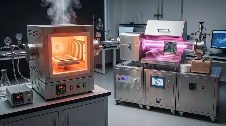
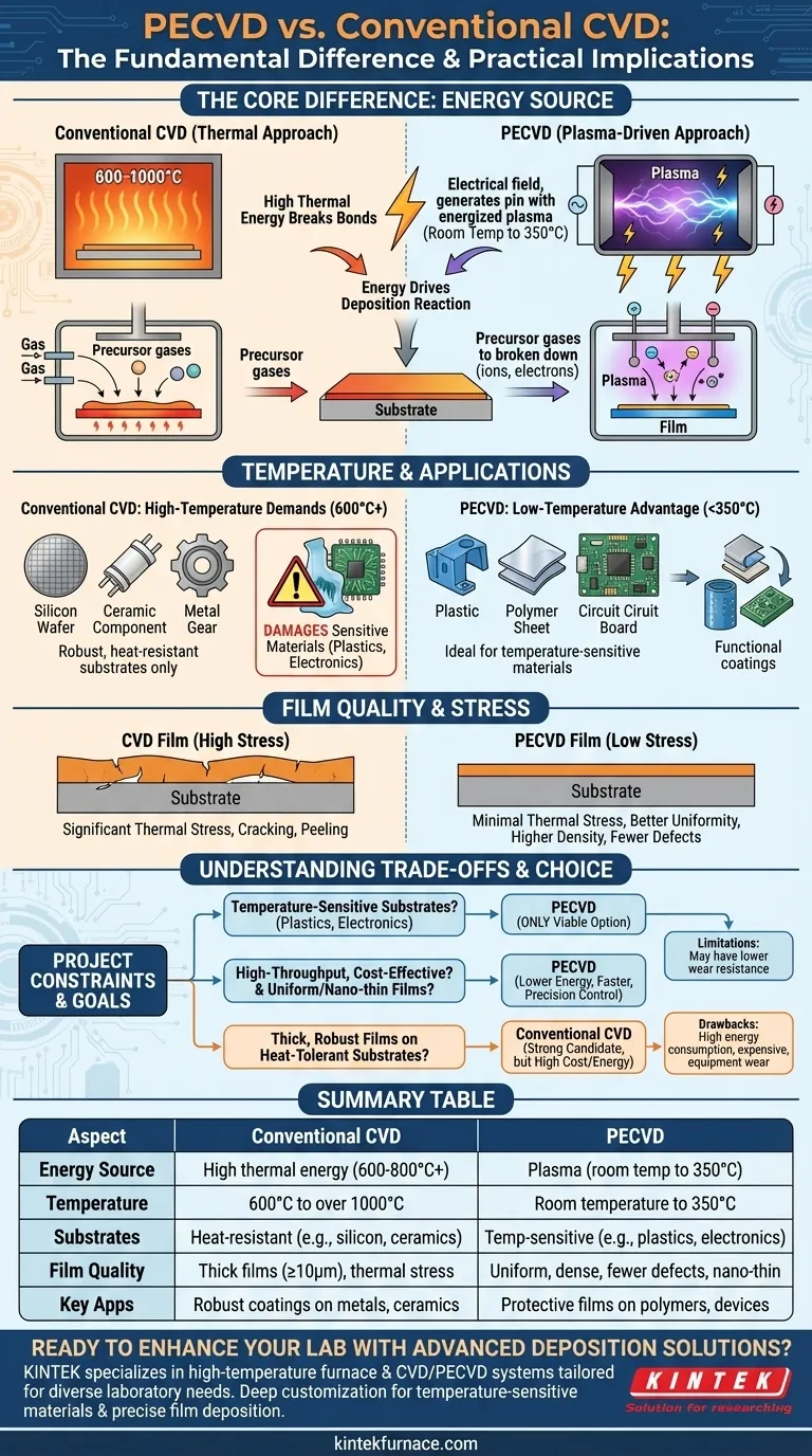
The fundamental difference between Plasma-Enhanced Chemical Vapor Deposition (PECVD) and conventional Chemical Vapor Deposition (CVD) is the energy source used to drive the reaction. Conventional CVD relies entirely on high heat (600-800°C) to break down precursor gases and deposit a film onto a substrate. In stark contrast, PECVD uses an energized plasma to achieve the same result at significantly lower temperatures (room temperature to 350°C).
The core distinction isn't just academic; it's practical. By replacing extreme heat with an energized plasma, PECVD opens the door to depositing high-quality thin films on temperature-sensitive materials like plastics, polymers, and complex electronics—a task that is often impossible with conventional CVD without causing damage.
The Core Mechanism: Thermal Energy vs. Plasma
The choice of energy source is the defining characteristic that separates these two deposition methods, dictating their capabilities, applications, and limitations.
Conventional CVD: The Thermal Approach
Conventional CVD operates much like a high-temperature oven. Precursor gases are introduced into a chamber where the substrate is heated to extremely high temperatures.
This thermal energy is what breaks the chemical bonds in the gases, allowing the desired elements to deposit and form a solid film on the substrate's surface.
PECVD: The Plasma-Driven Approach
PECVD replaces brute-force heat with a more sophisticated energy source: plasma. An electrical field is applied to the precursor gas, stripping electrons from atoms and creating a highly reactive mix of ions, electrons, and free radicals.
These high-energy particles in the plasma have enough energy to break chemical bonds and drive the deposition reaction. Because the energy is delivered by particles rather than ambient heat, the substrate itself can remain at a much lower temperature.
How Temperature Dictates Application
The radical difference in operating temperature is the most significant practical consequence, directly influencing which materials can be coated and the quality of the final film.
The High-Temperature Demands of CVD
With typical temperatures ranging from 600°C to over 1000°C, conventional CVD is restricted to coating robust, heat-resistant substrates like silicon wafers, ceramics, or metals.
Attempting to use CVD on a plastic component or a fully assembled electronic device would lead to melting, warping, or complete destruction of the substrate.
The Low-Temperature Advantage of PECVD
PECVD's low process temperatures (typically under 350°C) make it uniquely suitable for temperature-sensitive materials.
This allows for the deposition of protective or functional coatings on polymers, plastics, and even complex devices with pre-existing electronic components, vastly expanding the range of possible applications.
Impact on Film Quality and Stress
High temperatures can induce significant thermal stress in a growing film, which may lead to cracking, peeling, or a mismatch with the substrate's crystal lattice.
PECVD's low-temperature environment minimizes this thermal stress, often resulting in films with better uniformity, higher density, and fewer pinholes or defects.
Understanding the Trade-offs
While PECVD's low-temperature process offers significant advantages, the choice is not always straightforward. Each method has distinct limitations.
Limitations of PECVD
PECVD films can sometimes exhibit lower performance in specific areas. They may have limited wear resistance due to being softer than high-temperature CVD films.
Furthermore, their performance as a barrier can be weaker than specialized coatings like Parylene, and the use of certain precursors (like halogenated gases) can introduce potential health or environmental concerns.
Drawbacks of Conventional CVD
The primary drawbacks of CVD are its high energy consumption and operational cost, driven by the need for prolonged high temperatures and often expensive precursors.
The intense heat also causes wear and tear on the equipment itself, limiting its operational life. Finally, CVD is generally used for creating relatively thick films (10µm or more) and lacks the precision for producing functional nano-thin layers.
Making the Right Choice for Your Project
Your choice between PECVD and CVD depends entirely on your project's specific constraints and desired outcomes.
- If your primary focus is coating temperature-sensitive substrates like plastics or electronics: PECVD is your only viable option due to its low-temperature process.
- If your primary focus is high-throughput, cost-effective production: PECVD generally offers lower energy costs, faster deposition rates, and higher automation flexibility.
- If your primary focus is creating very thick, robust films on a heat-tolerant substrate: Conventional CVD remains a strong and well-established candidate, despite its higher temperature and cost.
- If your primary focus is depositing highly uniform, nano-thin, or functionally tailored films: PECVD provides superior control for creating films with specific properties like hydrophobicity or UV protection at thicknesses of 50nm or more.
Ultimately, understanding this core difference in energy sources empowers you to select the precise tool required for your specific material and performance goals.
Summary Table:
| Aspect | Conventional CVD | PECVD |
|---|---|---|
| Energy Source | High thermal energy (600-800°C+) | Plasma (room temp to 350°C) |
| Temperature Range | 600°C to over 1000°C | Room temperature to 350°C |
| Suitable Substrates | Heat-resistant (e.g., silicon, ceramics) | Temperature-sensitive (e.g., plastics, electronics) |
| Film Quality | Thick films (≥10µm), potential thermal stress | Uniform, dense, fewer defects, nano-thin layers |
| Key Applications | Robust coatings on metals, ceramics | Protective films on polymers, complex devices |
Ready to enhance your lab's capabilities with advanced deposition solutions? KINTEK specializes in high-temperature furnace systems, including CVD/PECVD systems, tailored for diverse laboratory needs. Leveraging our exceptional R&D and in-house manufacturing, we offer deep customization to meet your unique experimental requirements—whether you're working with temperature-sensitive materials or need precise film deposition. Contact us today to discuss how our solutions can drive your research forward!
Visual Guide
Related Products
- Slide PECVD Tube Furnace with Liquid Gasifier PECVD Machine
- RF PECVD System Radio Frequency Plasma Enhanced Chemical Vapor Deposition
- Inclined Rotary Plasma Enhanced Chemical Deposition PECVD Tube Furnace Machine
- Inclined Rotary Plasma Enhanced Chemical Deposition PECVD Tube Furnace Machine
- Multi Heating Zones CVD Tube Furnace Machine for Chemical Vapor Deposition Equipment
People Also Ask
- How does a hydrogen reduction environment in an industrial tube furnace facilitate gold-copper alloy microspheres?
- What plasma source is used in PE-CVD tube furnaces? Unlock Low-Temperature, High-Quality Deposition
- What are the advantages of using a tube furnace CVD system for Cu(111)/graphene? Superior Scalability and Quality
- What are the typical conditions for plasma-enhanced CVD processes? Achieve Low-Temperature Thin Film Deposition
- What are the disadvantages of tube furnace cracking when processing heavy raw materials? Avoid Costly Downtime and Inefficiency


