In short, Plasma-Enhanced Chemical Vapor Deposition (PECVD) is a cornerstone technology used to create high-performance thin films. These films are essential for manufacturing a vast range of products, including semiconductors, solar cells, optical lenses, and protective coatings for medical devices and even food packaging.
The core challenge in modern fabrication is depositing high-quality, functional layers onto substrates without damaging them with extreme heat. PECVD solves this by using an energized gas, or plasma, to drive the chemical reaction, enabling a low-temperature process that is both precise and incredibly versatile.
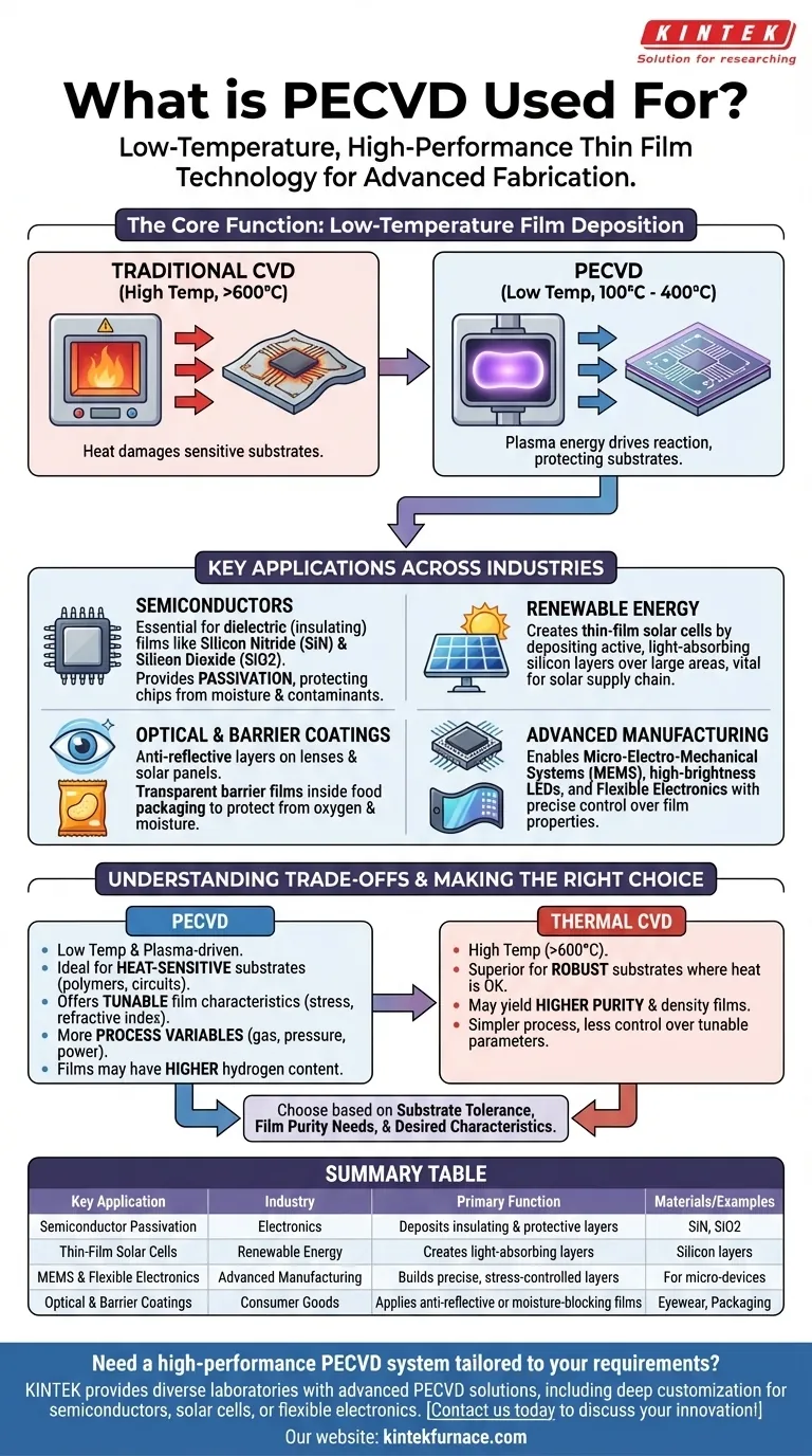
The Core Function: Low-Temperature Film Deposition
At its heart, PECVD is a process for turning a gas into a solid, ultra-thin layer on a surface. Its unique advantage over other methods lies in how it achieves this transformation.
The Plasma Advantage
Traditional Chemical Vapor Deposition (CVD) relies on very high temperatures (often >600°C) to provide the energy needed for reactant gases to form a solid film.
PECVD, by contrast, creates a plasma by applying an electric field to the gas. This plasma provides the necessary energy to initiate the chemical reaction, allowing deposition to occur at much lower temperatures, typically between 100°C and 400°C.
Why Low Temperature is a Game-Changer
The ability to deposit films at low temperatures is the key to PECVD's widespread use. It allows manufacturers to coat materials that would otherwise melt, warp, or be destroyed by high-heat processes.
This opens up fabrication possibilities for heat-sensitive substrates like plastics, flexible polymers, and, critically, complex semiconductor wafers that already contain previously fabricated electronic circuits.
Key Applications Across Industries
PECVD's unique capability makes it indispensable in several high-tech fields. It isn't just one application, but a foundational process that enables countless others.
The Foundation of Modern Electronics
In the semiconductor industry, PECVD is a workhorse. It is used to deposit critical dielectric (insulating) films, such as silicon nitride (SiN) and silicon dioxide (SiO2).
These layers isolate conductive pathways from each other within an integrated circuit, form capacitors, and provide passivation—a final protective coating that shields the delicate chip from moisture and contaminants.
Powering Renewable Energy
PECVD is essential for the production of thin-film solar cells. The process is used to deposit the layers of silicon that form the active, light-absorbing region of the photovoltaic cell.
Its ability to create high-quality films over large areas cost-effectively makes it a vital part of the solar energy supply chain.
Enhancing Material Performance
The technology is widely used to create functional coatings that improve the properties of a surface.
This includes optical coatings, such as anti-reflective layers on eyeglass lenses and solar panels, and barrier coatings, like the thin, transparent film inside a potato chip bag that protects it from oxygen and moisture. It is also used for hard, wear-resistant coatings on tools and medical implants.
Enabling Next-Generation Devices
For advanced manufacturing, PECVD's precision is critical. It is used to build Micro-Electro-Mechanical Systems (MEMS), high-brightness LEDs, and components for flexible electronics. The precise control over film thickness, composition, and stress is essential for these sophisticated devices to function correctly.
Understanding the Trade-offs
While incredibly powerful, PECVD is not a universal solution. Understanding its limitations is key to using it effectively.
Film Quality vs. Thermal CVD
Because PECVD operates at lower temperatures and uses plasma, the resulting films can have different properties than those from high-temperature thermal CVD. For instance, PECVD films often contain a higher concentration of hydrogen.
For applications demanding the absolute highest film purity and density, a high-temperature process might be superior, but only if the substrate can withstand the heat.
Process Complexity
Managing a plasma introduces more variables than a simple thermal process. Achieving the desired film properties requires precise control over gas flow, pressure, chamber temperature, and the frequency and power of the electric field. This complexity requires significant process engineering and expertise.
Making the Right Choice for Your Goal
Your choice of deposition method depends entirely on the requirements of your substrate and final product.
- If your primary focus is depositing films on heat-sensitive materials like polymers or finished circuits: PECVD is the industry-standard solution due to its low-temperature processing capabilities.
- If your primary focus is achieving the highest possible film purity and density on a robust substrate: You should also evaluate high-temperature thermal CVD, as it may yield superior material properties if heat is not a constraint.
- If your primary focus is engineering specific film characteristics like stress or refractive index: PECVD offers a wide range of tunable parameters (power, pressure, gas mix) that provide exceptional control over the final film.
Ultimately, PECVD is a foundational technology that enables the creation of complex devices that would be impossible to fabricate with high-heat methods alone.
Summary Table:
| Key Application | Industry | Primary Function |
|---|---|---|
| Semiconductor Passivation | Electronics | Deposits insulating layers (SiN, SiO2) to protect chips |
| Thin-Film Solar Cells | Renewable Energy | Creates light-absorbing silicon layers for photovoltaics |
| MEMS & Flexible Electronics | Advanced Manufacturing | Builds precise, stress-controlled layers for micro-devices |
| Optical & Barrier Coatings | Consumer Goods | Applies anti-reflective or moisture-blocking films |
Need a high-performance PECVD system tailored to your unique requirements?
Leveraging exceptional R&D and in-house manufacturing, KINTEK provides diverse laboratories with advanced PECVD solutions. Our product line, including CVD/PECVD Systems, is complemented by strong deep customization capability to precisely meet your experimental needs—whether for semiconductors, solar cells, or flexible electronics.
Contact us today to discuss how our PECVD technology can accelerate your innovation!
Visual Guide
Related Products
- Slide PECVD Tube Furnace with Liquid Gasifier PECVD Machine
- RF PECVD System Radio Frequency Plasma Enhanced Chemical Vapor Deposition
- Inclined Rotary Plasma Enhanced Chemical Deposition PECVD Tube Furnace Machine
- Inclined Rotary Plasma Enhanced Chemical Deposition PECVD Tube Furnace Machine
- Multi Heating Zones CVD Tube Furnace Machine for Chemical Vapor Deposition Equipment
People Also Ask
- What are the typical conditions for plasma-enhanced CVD processes? Achieve Low-Temperature Thin Film Deposition
- What are the disadvantages of tube furnace cracking when processing heavy raw materials? Avoid Costly Downtime and Inefficiency
- What is plasma in the context of PECVD? Unlock Low-Temperature Thin Film Deposition
- What role does a Tube Furnace play in the CVD growth of carbon nanotubes? Achieve High-Purity CNT Synthesis
- How does PECVD equipment contribute to TOPCon bottom cells? Mastering Hydrogenation for Maximum Solar Efficiency


