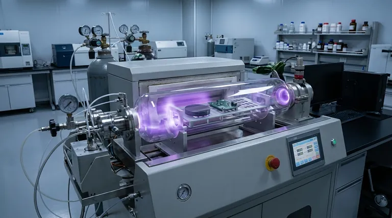
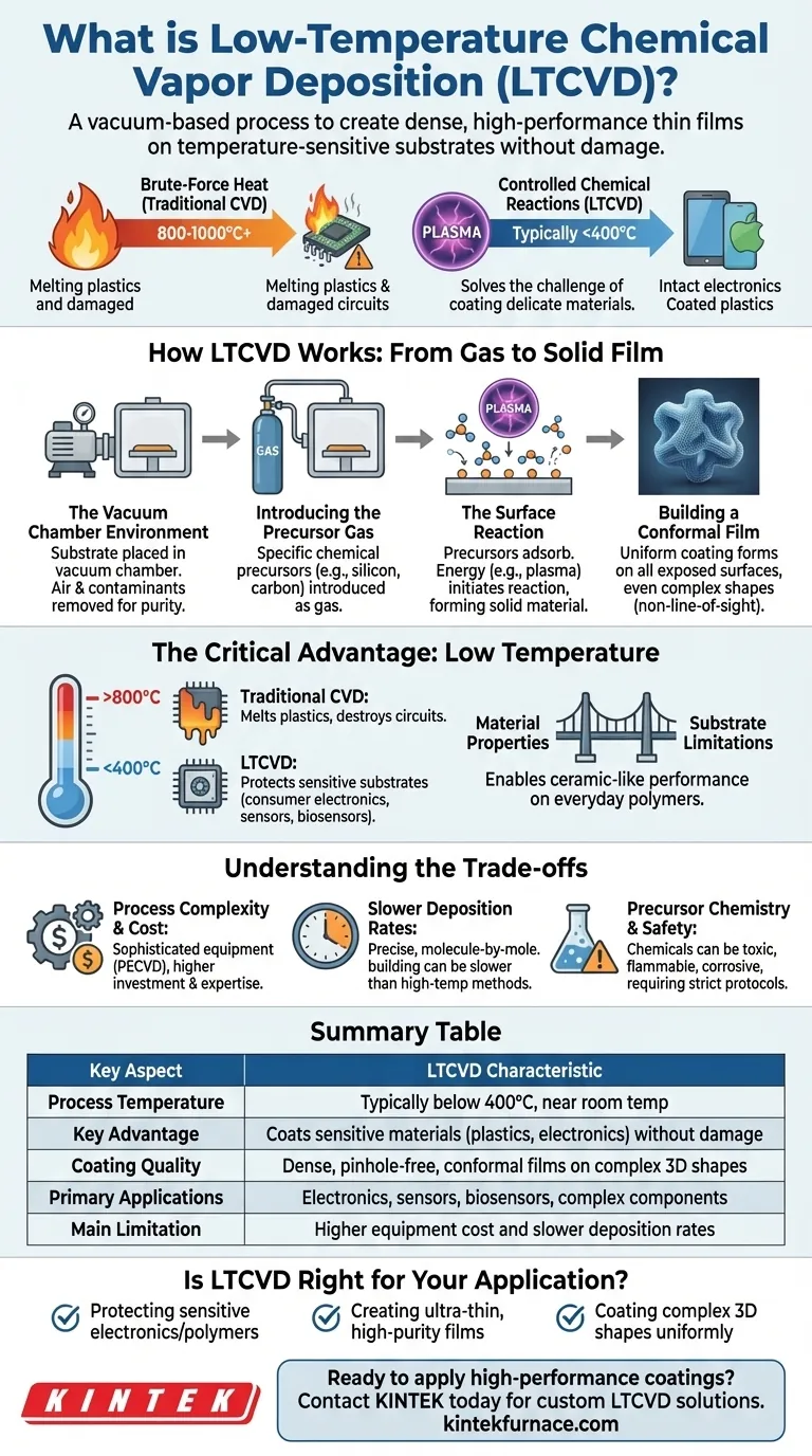
At its core, low-temperature chemical vapor deposition (LTCVD) is a vacuum-based process used to create exceptionally dense, high-performance thin films on a substrate. It works by introducing a vaporized chemical, known as a precursor, which then reacts and solidifies on the substrate's surface, building a protective coating molecule by molecule. The key is that this occurs at temperatures low enough to avoid damaging sensitive components like electronics or plastics.
The central challenge in modern manufacturing is applying high-performance coatings to temperature-sensitive materials. LTCVD solves this by replacing brute-force heat with controlled chemical reactions, enabling the creation of durable, ultra-thin films on delicate products.
How LTCVD Works: From Gas to Solid Film
To understand the value of LTCVD, you must first grasp its fundamental mechanism. The entire process takes place within a highly controlled vacuum chamber, which is critical for purity and process stability.
The Vacuum Chamber Environment
First, a substrate—the object to be coated—is placed inside a vacuum chamber. All air and contaminants are pumped out. This ensures that the only chemicals present are the ones we deliberately introduce, preventing unwanted reactions and ensuring a pure final film.
Introducing the Precursor Gas
Next, one or more chemical precursors are introduced into the chamber as a gas. These precursors are specifically chosen molecules that contain the atoms needed for the desired film (e.g., silicon, carbon, nitrogen).
The Surface Reaction
This is the heart of the process. The precursor gas molecules adsorb onto the surface of the substrate. Instead of using high heat to break them apart, LTCVD uses other energy sources, such as a plasma, to initiate a chemical reaction. This energy causes the precursors to decompose or react right on the surface, leaving behind a solid material and creating gaseous byproducts that are pumped away.
Building a Conformal Film, Molecule by Molecule
Because the process is driven by a gas that fills the entire chamber, the coating forms uniformly on all exposed surfaces. This non-line-of-sight deposition is a major advantage, as it perfectly coats complex 3D shapes, internal cavities, and intricate geometries where spraying or other line-of-sight methods would fail. The result is an extremely dense, pinhole-free film.
The Critical Advantage: "Low Temperature" Explained
The term "low temperature" is relative, but its impact is absolute. It is the single biggest factor that expands the applications for high-performance coatings.
Protecting Sensitive Substrates
Traditional CVD processes can require temperatures exceeding 800-1000°C, which would melt plastics and destroy integrated circuits. LTCVD operates at much lower temperatures, often below 400°C and sometimes near room temperature.
This allows for the deposition of robust ceramic or diamond-like coatings on fully assembled products, including consumer electronics, automotive sensors, and even biosensors, without damaging the delicate components inside.
Enabling High-Performance on Everyday Materials
LTCVD bridges the gap between material properties and substrate limitations. It makes it possible to give a plastic smartphone case the hardness of a ceramic or to protect a sensitive HVAC sensor from corrosion with an inert, ultra-thin layer.
This opens a vast range of design possibilities, combining the low cost and light weight of polymers with the durability and performance of advanced materials.
Understanding the Trade-offs
Like any advanced manufacturing process, LTCVD is not a universal solution. Understanding its limitations is key to making an informed decision.
Process Complexity and Equipment Cost
CVD systems, particularly those using plasma enhancement (PECVD), are sophisticated and expensive machines. They require significant capital investment and expertise to operate and maintain compared to simpler coating methods like painting or dipping.
Slower Deposition Rates
Building a film molecule by molecule is precise, but it can be slow. Lowering the temperature often reduces the reaction rate, which can lead to longer cycle times and lower manufacturing throughput compared to high-temperature alternatives.
Precursor Chemistry and Safety
The choice of precursor chemicals is critical to the film's final properties and is not limitless. These chemicals can be toxic, flammable, or corrosive, requiring stringent safety protocols and handling procedures.
Is LTCVD Right for Your Application?
Choosing a coating technology depends entirely on your specific goal, balancing performance requirements with material constraints and cost.
- If your primary focus is protecting sensitive electronics or polymers: LTCVD is an ideal solution for creating a robust environmental barrier without causing thermal damage to the underlying product.
- If your primary focus is creating ultra-thin, high-purity films for semiconductors: The atomic-level precision of LTCVD is a foundational technology for building the complex, multi-layered structures found in microchips.
- If your primary focus is coating complex 3D shapes uniformly: The non-line-of-sight nature of LTCVD ensures a perfectly conformal film on intricate geometries where no other method can succeed.
Ultimately, low-temperature chemical vapor deposition empowers you to apply the ideal material properties to virtually any product, regardless of its thermal sensitivity.
Summary Table:
| Key Aspect | LTCVD Characteristic |
|---|---|
| Process Temperature | Typically below 400°C, sometimes near room temperature |
| Key Advantage | Coats sensitive materials (plastics, electronics) without damage |
| Coating Quality | Dense, pinhole-free, conformal films on complex 3D shapes |
| Primary Applications | Electronics, sensors, biosensors, complex components |
| Main Limitation | Higher equipment cost and slower deposition rates |
Ready to apply high-performance coatings to your temperature-sensitive products?
At KINTEK, we leverage our exceptional R&D and in-house manufacturing capabilities to provide advanced LTCVD solutions tailored to your unique needs. Our product line, including specialized Vacuum & Atmosphere Furnaces and CVD/PECVD Systems, is complemented by strong deep customization capabilities to precisely meet your experimental and production requirements.
Whether you're working with delicate electronics, complex 3D components, or innovative polymer designs, we can help you achieve the perfect protective coating without compromising your substrate's integrity.
Contact our experts today to discuss how our LTCVD solutions can enhance your product performance and durability.
Visual Guide
Related Products
- MPCVD Machine System Reactor Bell-jar Resonator for Lab and Diamond Growth
- Custom Made Versatile CVD Tube Furnace Chemical Vapor Deposition CVD Equipment Machine
- 915MHz MPCVD Diamond Machine Microwave Plasma Chemical Vapor Deposition System Reactor
- Slide PECVD Tube Furnace with Liquid Gasifier PECVD Machine
- HFCVD Machine System Equipment for Drawing Die Nano Diamond Coating
People Also Ask
- Why is temperature control important in the MPCVD growth process? Ensure High-Quality, Reliable Diamond Film Deposition
- What are the advantages of MPCVD over LPCVD and PECVD? Achieve Superior Film Quality and Uniformity
- What are future trends in MPCVD technology? Unlock Next-Gen Materials with AI and Efficiency
- What role does gas flow rate play in MPCVD? Mastering Deposition Rate and Film Uniformity
- How can the growth rate of diamond be accelerated in the MPCVD method? Boost Growth with Higher Power & Pressure


