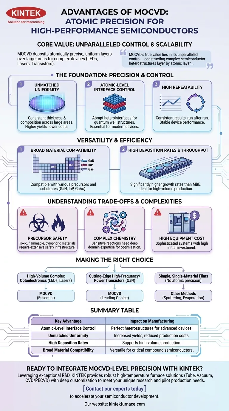
At its core, Metal-Organic Chemical Vapor Deposition (MOCVD) is the leading industrial process for manufacturing high-performance compound semiconductor devices. Its primary advantages are the ability to deposit atomically precise, highly uniform layers of material over large areas. This combination of fine control and scalability makes it indispensable for producing complex electronic and optoelectronic components like LEDs, laser diodes, and high-power transistors.
MOCVD's true value lies in its unparalleled control. It allows engineers to construct complex semiconductor heterostructures layer by atomic layer, achieving a level of precision and uniformity that is critical for the performance and mass production of modern electronic devices.
The Foundation: Precision and Control
The main advantages of MOCVD stem from its ability to precisely control the growth of thin films at the atomic level. This control is the reason it has become a cornerstone of the semiconductor industry.
Unmatched Uniformity Across Large Areas
MOCVD excels at depositing films with exceptionally uniform thickness and chemical composition. This consistency can be maintained across an entire large-area wafer.
This uniformity is not just a technical curiosity; it directly translates to higher manufacturing yields. When every device on a wafer performs identically, more chips are viable for sale, significantly reducing production costs.
Atomic-Level Interface Control
The technique allows for the creation of abrupt heterointerfaces, which are perfectly sharp transitions between different semiconductor materials.
Think of this as building with different types of LEGO bricks, where each layer clicks perfectly into place without any mixing. This capability is essential for fabricating advanced quantum well structures, which are the functional heart of modern laser diodes and high-efficiency LEDs.
High Degree of Repeatability
Once a process is dialed in, MOCVD delivers highly consistent results from one production run to the next. The precise digital control over gas flows and reaction conditions ensures that device characteristics remain stable over time.
This repeatability is critical for commercial manufacturing, where customers expect consistent performance from every component they purchase.
Versatility and Production Efficiency
Beyond precision, MOCVD is a highly practical and efficient manufacturing technology, adaptable to a wide range of needs.
Broad Material and Substrate Compatibility
MOCVD is not limited to a single material system. It is a highly versatile technique compatible with a vast library of precursor gases and substrates.
This allows it to be used for growing many of the most important compound semiconductors, including Gallium Nitride (GaN), Indium Phosphide (InP), and Gallium Arsenide (GaAs), which are the basis for RF electronics, fiber optics, and solid-state lighting.
High Deposition Rates for Throughput
Compared to other atomic-level deposition techniques like Molecular Beam Epitaxy (MBE), MOCVD generally offers significantly higher growth rates.
This efficiency means more wafers can be processed in less time, increasing factory throughput and further lowering the cost per device. This advantage is a key reason MOCVD dominates high-volume production for applications like general lighting.
Understanding the Trade-offs and Complexities
While powerful, MOCVD is not without its challenges. Its advantages come with significant operational complexities and costs.
Precursor Handling and Safety
The "metal-organic" precursors used in MOCVD are often highly toxic, flammable, and pyrophoric (igniting spontaneously in air). Handling these materials requires extensive safety infrastructure and rigorous protocols, adding to operational overhead.
Complex Chemistry and Optimization
The chemical reactions inside an MOCVD reactor are incredibly complex and sensitive to small changes in temperature, pressure, and gas flow dynamics. Optimizing a new process can be a time-consuming and expensive endeavor requiring deep domain expertise.
High Initial Equipment Cost
MOCVD reactors are sophisticated and expensive systems. The high capital investment required can be a barrier to entry, especially when compared to simpler thin-film deposition methods like sputtering or evaporation.
Making the Right Choice for Your Application
Selecting a deposition technology depends entirely on your final goal. MOCVD is a specialized tool that excels in specific domains.
- If your primary focus is high-volume production of complex optoelectronics (like LEDs or lasers): MOCVD's combination of uniformity, throughput, and atomic-level control is virtually essential.
- If your primary focus is fabricating cutting-edge high-frequency or high-power transistors: The ability to create perfect heterostructures makes MOCVD a leading choice for materials like GaN.
- If your primary focus is depositing simple, single-material films where atomic precision is not critical: Other methods like sputtering or thermal evaporation are often more cost-effective and simpler to operate.
Ultimately, MOCVD is the technology of choice when the performance of your device is directly tied to the perfection of its atomic structure.
Summary Table:
| Key Advantage | Impact on Semiconductor Manufacturing |
|---|---|
| Atomic-Level Interface Control | Enables creation of perfect heterostructures for advanced laser diodes and quantum well devices |
| Unmatched Uniformity Across Large Areas | Increases manufacturing yield and reduces production costs for consistent device performance |
| High Deposition Rates & Throughput | Supports high-volume production for applications like solid-state lighting and RF electronics |
| Broad Material Compatibility | Versatile for growing GaN, InP, GaAs and other critical compound semiconductors |
Ready to Integrate MOCVD-Level Precision into Your Lab?
Leveraging exceptional R&D and in-house manufacturing, KINTEK provides semiconductor and advanced materials laboratories with robust high-temperature furnace solutions. Our product line, including advanced Tube Furnaces, Vacuum & Atmosphere Furnaces, and CVD/PECVD Systems, is complemented by our strong deep customization capability to precisely meet your unique research and pilot production requirements.
Contact our experts today to discuss how our customized thermal solutions can accelerate your semiconductor development.
Visual Guide
Related Products
- Multi Heating Zones CVD Tube Furnace Machine for Chemical Vapor Deposition Equipment
- 915MHz MPCVD Diamond Machine Microwave Plasma Chemical Vapor Deposition System Reactor
- Molybdenum Disilicide MoSi2 Thermal Heating Elements for Electric Furnace
- Multi Zone Laboratory Quartz Tube Furnace Tubular Furnace
- Molybdenum Vacuum Heat Treat Furnace
People Also Ask
- What role do multi zone tube furnaces play in new energy research? Unlock Precise Thermal Control for Innovation
- What are the main applications of multi zone tube furnaces in university laboratories? Unlock Precision in Material Science and Energy Research
- Why are multi zone tube furnaces particularly useful for nanomaterial research? Unlock Precise Thermal Control for Advanced Synthesis
- How are multi zone tube furnaces used in ceramics, metallurgy and glass research? Unlock Precise Thermal Control for Advanced Materials
- What are the advantages of multi-zone tube furnaces? Achieve Superior Thermal Control for Advanced Materials Processing