At its core, chemical vapor deposition (CVD) is a method for "growing" solid materials from a gas. It is a vacuum-based process where chemical precursors in a vapor state are introduced into a reaction chamber. These gases then decompose or react on the surface of a substrate (the object to be coated), forming a highly pure, solid thin film atom by atom.
While often perceived as a coating technique, CVD is more accurately a material synthesis process. Its true value is the ability to construct ultra-pure, high-performance thin films with atomic-level precision, making it indispensable for modern electronics and advanced materials.
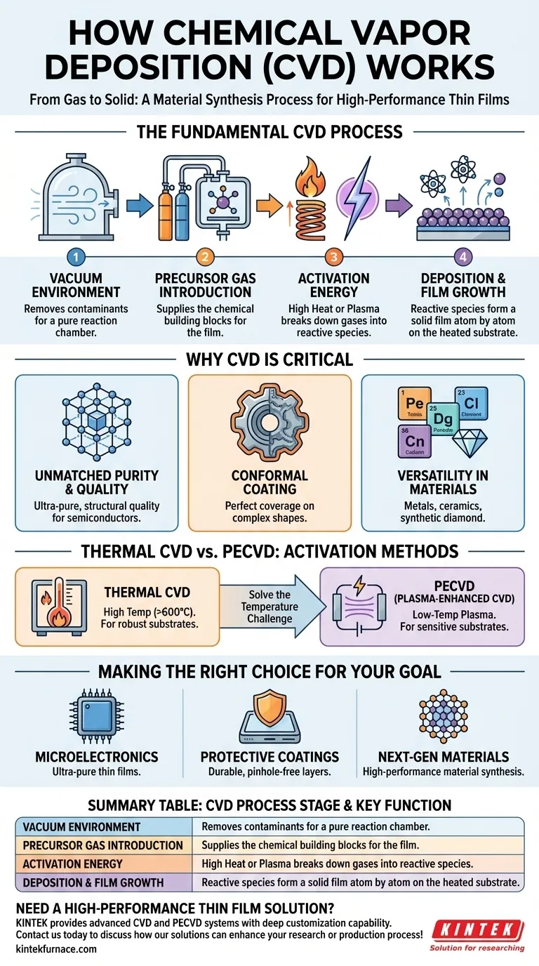
The Fundamental CVD Process: From Gas to Solid
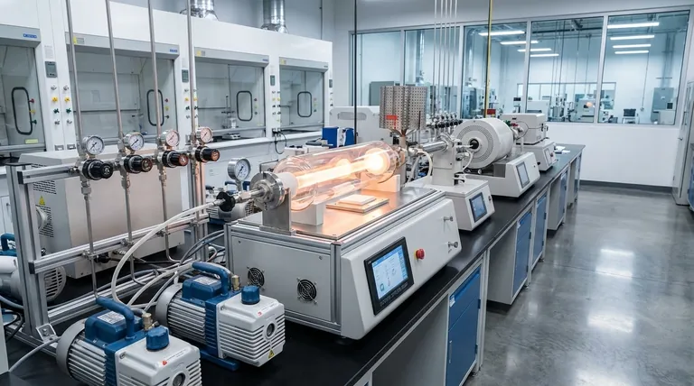
To understand how CVD works, it's best to break it down into its essential stages. The entire process takes place inside a controlled vacuum chamber to ensure purity and prevent unwanted reactions.
The Vacuum Environment
The first step is creating a vacuum. This removes air and other potential contaminants from the chamber, ensuring that the only chemicals present are the ones intentionally introduced for the deposition.
Introducing Precursor Gases
Next, one or more volatile precursor gases are fed into the chamber. These gases contain the atoms required for the final film—for example, a silicon-containing gas might be used to deposit a silicon film.
The Activation Energy
The precursor gases do not react on their own. They must be activated with energy, which causes them to break down (decompose) and become reactive. This energy is typically supplied by high heat, but other methods like plasma can also be used.
Deposition and Film Growth
Once activated, the reactive chemical species adsorb onto the heated substrate surface. They then form a stable, solid film, releasing any volatile byproducts which are pumped out of the chamber. Because this happens molecule by molecule, the resulting film is extremely uniform and dense.
Why CVD is Critical for Modern Technology
The precision and control offered by CVD make it a foundational process in high-tech manufacturing, especially for products that rely on micro-scale performance.
Unmatched Purity and Quality
The vacuum environment and controlled chemical reactions produce thin films of exceptionally high purity and structural quality. This is non-negotiable for applications like semiconductor manufacturing, where even tiny impurities can ruin a microchip.
Conformal Coating
Because the material is built up from a gas phase, CVD can deposit a perfectly uniform layer over complex, three-dimensional shapes. This "conformal" coating ensures complete coverage without the weaknesses or gaps that liquid-based coatings can leave behind.
Versatility in Materials
The process is incredibly versatile. By changing the precursor gases and process conditions, CVD can be used to deposit a vast range of materials, including metals, ceramics (like silicon nitride), and even advanced materials like synthetic diamond.
Understanding the Trade-offs and Variations
While powerful, the standard CVD process has limitations. Understanding these has led to important variations that broaden its applicability.
The Challenge of High Temperatures
Traditional thermal CVD often requires very high temperatures (often >600°C) to activate the precursor gases. This can damage sensitive substrates, such as plastics or fully fabricated electronic components.
The Plasma Solution (PECVD)
Plasma-Enhanced CVD (PECVD) is a key variation that solves the temperature problem. In PECVD, an electric field creates a low-temperature plasma (an ionized gas) inside the chamber. This plasma provides the energy to break down the precursor gases, allowing deposition to occur at much lower temperatures.
Process Complexity
CVD systems are sophisticated machines requiring precise control over vacuum levels, gas flow rates, and temperature. This makes the process more complex and costly than simpler coating methods, reserving its use for applications where high performance is paramount.
Making the Right Choice for Your Goal
The decision to use CVD depends entirely on the technical requirements of the final product.
- If your primary focus is mass-producing microelectronics: CVD is the industry standard for depositing the ultra-pure, uniform thin films essential for fabricating transistors and interconnects.
- If your primary focus is creating durable, protective coatings: CVD and PECVD provide dense, pinhole-free layers that protect sensitive devices like automotive sensors and medical implants from corrosion and wear.
- If your primary focus is developing next-generation materials: The versatility of CVD allows for the synthesis of high-performance materials, such as synthetic diamond for cutting tools or advanced dielectrics for future electronics.
Ultimately, understanding chemical vapor deposition is to understand the atomic-level engineering that builds the foundation of our modern technological world.
Summary Table:
| CVD Process Stage | Key Function |
|---|---|
| Vacuum Environment | Removes contaminants for a pure reaction chamber. |
| Precursor Gas Introduction | Supplies the chemical building blocks for the film. |
| Activation (Heat/Plasma) | Provides energy to decompose gases into reactive species. |
| Deposition & Growth | Reactive species form a solid film on the substrate surface. |
Need a high-performance thin film solution?
Leveraging exceptional R&D and in-house manufacturing, KINTEK provides diverse laboratories with advanced CVD and PECVD systems. Our product line, including Tube Furnaces, Vacuum & Atmosphere Furnaces, and specialized CVD/PECVD Systems, is complemented by our strong deep customization capability to precisely meet your unique material synthesis and coating requirements.
Contact us today to discuss how our solutions can enhance your research or production process!
Visual Guide
Related Products
- Custom Made Versatile CVD Tube Furnace Chemical Vapor Deposition CVD Equipment Machine
- MPCVD Machine System Reactor Bell-jar Resonator for Lab and Diamond Growth
- Multi Heating Zones CVD Tube Furnace Machine for Chemical Vapor Deposition Equipment
- 915MHz MPCVD Diamond Machine Microwave Plasma Chemical Vapor Deposition System Reactor
- Slide PECVD Tube Furnace with Liquid Gasifier PECVD Machine
People Also Ask
- What is a CVD tube furnace and what is its primary function? Discover Precision Thin-Film Deposition
- Which industries and research fields benefit from CVD tube furnace sintering systems for 2D materials? Unlock Next-Gen Tech Innovations
- How can integrating CVD tube furnaces with other technologies benefit device fabrication? Unlock Advanced Hybrid Processes
- What customization options are available for CVD tube furnaces? Tailor Your System for Superior Material Synthesis
- What improvements can be made to the bonding force of gate dielectric films using a CVD tube furnace? Enhance Adhesion for Reliable Devices


