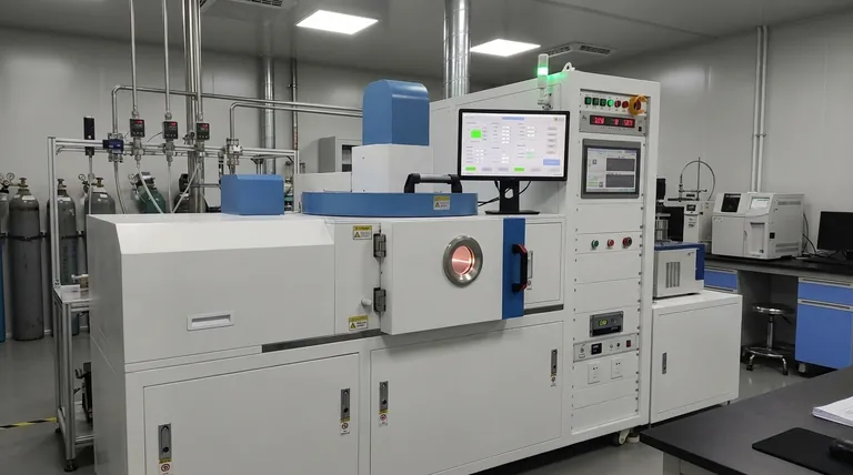
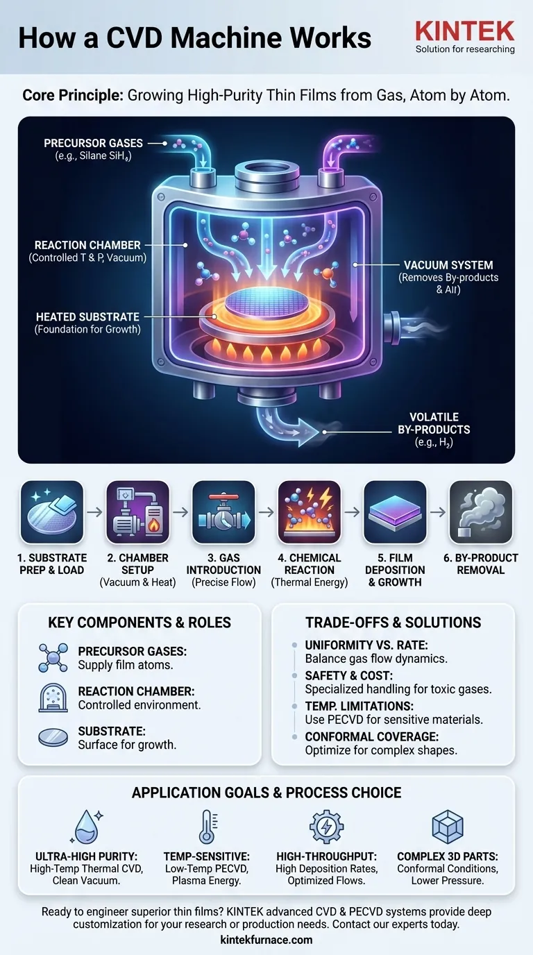
At its core, a Chemical Vapor Deposition (CVD) machine is a sophisticated chemical reactor designed to build a solid, high-purity thin film on top of a surface, known as a substrate. The machine introduces specific gaseous molecules, called precursors, into a controlled chamber. By precisely managing conditions like temperature and pressure, it triggers a chemical reaction that causes the precursors to decompose and deposit the desired material onto the substrate, forming a new layer atom by atom.
A CVD system doesn't simply coat a surface; it grows a new material layer directly onto it from a gas phase. This foundational principle is what enables the precise control over a film's thickness, composition, and physical properties that makes the technology so powerful.
The Fundamental Principle: Building from Gas
A CVD process is fundamentally about transforming a gas into a solid film within a highly controlled environment. Understanding the three key components is essential.
The Precursor: The Gaseous Building Blocks
A precursor is a volatile gas compound that contains the atoms you wish to deposit. For example, to create a film of pure silicon, you might use silane gas (SiH₄) as the precursor. The system's gas injectors carefully meter these precursors into the chamber.
The Reaction Chamber: The Controlled Environment
The entire process takes place inside a sealed reaction chamber. This chamber allows for the precise control of the two most critical variables: temperature and pressure. It is often operated under a vacuum to remove unwanted air and contaminants that could interfere with the chemical reaction.
The Substrate: The Foundation for Growth
The substrate is the material or object that you intend to coat. This could be a silicon wafer for a computer chip, a medical implant, or a cutting tool. The substrate is heated to provide the energy needed to drive the chemical reaction on its surface.
A Step-by-Step Breakdown of the Process
While there are many variations of CVD, they all follow a similar operational sequence to achieve the final, high-quality film.
Step 1: Substrate Preparation and Loading
The substrate is meticulously cleaned to remove any contaminants. It is then loaded into the reaction chamber, which is sealed shut.
Step 2: Chamber Environment Setup
The chamber is pumped down to a specific low pressure, or vacuum. The substrate and/or the chamber walls are then heated to the target reaction temperature, which can range from a few hundred to over a thousand degrees Celsius.
Step 3: Precursor Gas Introduction
Once the chamber environment is stable, a precise flow of one or more precursor gases is introduced. The flow rate is critical as it determines the availability of the "building block" atoms.
Step 4: The Chemical Reaction
Driven by the thermal energy from the heated substrate, the precursor gases react. They may decompose directly on the substrate's surface or react in the gas phase just above it, breaking their chemical bonds.
Step 5: Film Deposition and Growth
The freed atoms from the decomposed precursor then bond to the substrate's surface. This process repeats continuously, building up a thin, uniform, and solid film one atomic layer at a time.
Step 6: By-product Removal
The chemical reaction also produces unwanted volatile by-products (for example, the hydrogen gas from the silane precursor). These waste gases are continuously removed from the chamber by the vacuum system's exhaust.
Understanding the Trade-offs and Pitfalls
While powerful, CVD technology involves critical trade-offs and potential challenges that must be managed for successful outcomes.
Uniformity vs. Growth Rate
Achieving a perfectly uniform film across a large or complex substrate requires careful management of gas flow dynamics. Pushing for a very high growth rate by increasing precursor concentration can sometimes lead to non-uniformity or poor film quality.
Precursor Safety and Cost
Many precursor gases are highly toxic, flammable, or pyrophoric (igniting on contact with air). They require specialized storage, handling, and safety systems, which adds to the operational complexity and cost.
Substrate Temperature Limitations
Traditional thermal CVD relies on high temperatures to drive the reaction. This makes it unsuitable for coating temperature-sensitive materials like plastics or certain electronic components. This limitation has led to the development of other methods, like Plasma-Enhanced CVD (PECVD), which use an energy-rich plasma to enable reactions at much lower temperatures.
Conformal Coverage on Complex Shapes
One of CVD's great strengths is its ability to deposit a uniform "conformal" coating over intricate geometries. However, in very deep or narrow trenches, the precursor gas can be depleted before it reaches the bottom, a phenomenon that requires careful process tuning to overcome.
Applying This to Your Goal
Your specific objective determines which process parameters you need to prioritize.
- If your primary focus is ultra-high purity and crystalline quality: You will need high-temperature thermal CVD, extremely pure precursor gases, and a very clean, high-vacuum environment.
- If your primary focus is coating temperature-sensitive materials: You must use a low-temperature variant like Plasma-Enhanced CVD (PECVD) to avoid damaging your substrate.
- If your primary focus is high-throughput industrial production: You will need to optimize for high deposition rates by tuning gas flows and pressure, potentially accepting minor trade-offs in film uniformity.
- If your primary focus is coating complex 3D parts: You must prioritize process conditions that ensure conformal coverage, such as lower pressures that allow gas molecules to move more freely.
By understanding these core principles, you can effectively leverage Chemical Vapor Deposition to engineer materials with precision.
Summary Table:
| Key Component | Role in the CVD Process |
|---|---|
| Precursor Gases | Supply the atoms needed to build the film. |
| Reaction Chamber | Provides a controlled environment for temperature and pressure. |
| Substrate | The surface on which the new material layer is grown. |
| Process Steps | What Happens |
| 1. Preparation | Substrate is cleaned and chamber is evacuated. |
| 2. Heating | Substrate is heated to the required reaction temperature. |
| 3. Gas Introduction | Precursor gases are introduced into the chamber. |
| 4. Reaction & Deposition | Gases react/decompose, depositing a solid film on the substrate. |
| 5. By-product Removal | Waste gases are continuously pumped out of the chamber. |
Ready to engineer superior thin films for your specific application? Whether your goal is ultra-high purity, coating temperature-sensitive materials, or achieving conformal coverage on complex 3D parts, KINTEK's advanced CVD and PECVD systems are the solution. Leveraging our exceptional R&D and in-house manufacturing, we provide deep customization to precisely meet your unique research or production requirements.
Contact our experts today to discuss how our CVD technology can accelerate your innovation.
Visual Guide
Related Products
- 915MHz MPCVD Diamond Machine Microwave Plasma Chemical Vapor Deposition System Reactor
- Custom Made Versatile CVD Tube Furnace Chemical Vapor Deposition CVD Equipment Machine
- HFCVD Machine System Equipment for Drawing Die Nano Diamond Coating
- Cylindrical Resonator MPCVD Machine System for Lab Diamond Growth
- Split Chamber CVD Tube Furnace with Vacuum Station CVD Machine
People Also Ask
- What is the purpose of a microwave plasma chemical vapor deposition system? Grow High-Purity Diamonds and Advanced Materials
- In which industries is the microwave plasma chemical vapor deposition system commonly used? Unlock High-Purity Material Synthesis
- What are the main components of an MPCVD machine? Unlock the Secrets of Diamond Synthesis
- How does the MPCVD process work to deposit diamond? A Guide to High-Purity Synthesis
- What are some key features and benefits of the microwave plasma chemical vapor deposition system? Achieve Unmatched Material Synthesis


