The addition of silver nanoparticles acts as a critical "nano-solder" that fundamentally repairs structural imperfections. By introducing these microscopic particles into the Ag2Se composite, you enable a physical bridging process during heating that creates robust electrical connections between grains, drastically enhancing the material's overall utility.
Core Takeaway Due to their diminished size, silver nanoparticles possess a lower melting point than bulk material. This unique property allows them to melt and flow into micro-voids between Ag2Se grains during annealing, creating a dense, conductive network that significantly boosts the thermoelectric power factor.
The Mechanism of Improvement
The "Nano-Solder" Effect
The primary driver of performance improvement is the reduced melting point of the silver nanoparticles.
Because the particles are so small, they transition to a liquid or semi-liquid state at temperatures that leave the bulk material intact.
This allows the silver to act like solder, flowing effectively into the microscopic spaces within the film structure.
Filling Micro-Voids
In standard printed films, microscopic gaps—or micro-voids—naturally exist between Ag2Se grains.
These voids typically act as barriers to electricity, increasing resistance and hindering performance.
The molten silver nanoparticles fill these voids, physically cementing the grains together.
Establishing Robust Connections
Once the voids are filled, the film transitions from a collection of loose grains to a unified, cohesive structure.
This creates robust electrical connections throughout the composite.
The result is a continuous path for electrical current, bypassing the structural interruptions that previously limited the film's efficiency.
Impact on Performance Metrics
Reduction in Resistance
The direct consequence of filling micro-voids is a sharp decrease in the film's electrical resistance.
By removing the physical gaps between grains, the electrons encounter fewer obstacles as they traverse the material.
Enhanced Carrier Dynamics
The structural integration leads to measurable improvements in carrier concentration and mobility.
Electrons can move more freely and in greater numbers across the connected grains.
This optimization of electron flow is the primary contributor to the reported increase in the thermoelectric power factor.
Understanding the Process Constraints
The Necessity of High-Temperature Annealing
It is critical to note that the addition of nanoparticles alone is insufficient to achieve these results.
The process requires a high-temperature laboratory furnace to trigger the melting effect.
Without this specific thermal processing step, the nanoparticles would remain solid, failing to fill the voids or improve the electrical connections.
Making the Right Choice for Your Goal
To effectively utilize Ag2Se composite thin films, consider how this processing step aligns with your objectives:
- If your primary focus is maximizing thermoelectric power: Prioritize the inclusion of silver nanoparticles and ensure your fabrication process includes a high-temperature annealing phase to activate the "solder" effect.
- If your primary focus is minimizing electrical resistance: Focus on the granular structure of your film; the nanoparticles are essential for bridging the micro-voids that cause high impedance.
The integration of silver nanoparticles transforms a discontinuous film into a high-performance composite by physically healing the gaps between grains.
Summary Table:
| Feature | Impact of Silver Nanoparticles | Performance Result |
|---|---|---|
| Structural Voids | Fills micro-voids during annealing | Increases film density |
| Electrical Path | Creates robust inter-grain connections | Lowers electrical resistance |
| Carrier Dynamics | Optimizes mobility and concentration | Higher power factor |
| Melting Point | Lowered due to nano-size effects | Enables 'nano-solder' mechanism |
Elevate Your Thermoelectric Research with KINTEK Precision
Achieving the perfect 'nano-solder' effect in Ag2Se composites requires precise thermal control that only high-performance laboratory equipment can provide. KINTEK delivers the advanced heating solutions necessary for critical annealing processes.
Backed by expert R&D and manufacturing, KINTEK offers a comprehensive range of Muffle, Tube, Rotary, Vacuum, and CVD systems, as well as other lab high-temperature furnaces—all fully customizable to meet your unique material science needs.
Ready to optimize your thin film performance? Contact our experts today to find the ideal furnace for your laboratory.
References
- Yan Liu, Wan Jiang. Fully inkjet-printed Ag2Se flexible thermoelectric devices for sustainable power generation. DOI: 10.1038/s41467-024-46183-1
This article is also based on technical information from Kintek Furnace Knowledge Base .
Related Products
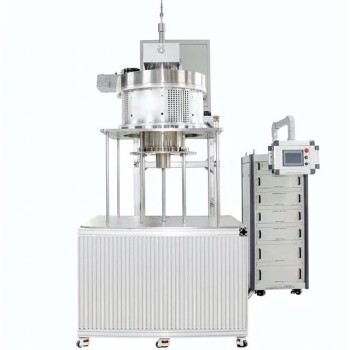
- 915MHz MPCVD Diamond Machine Microwave Plasma Chemical Vapor Deposition System Reactor
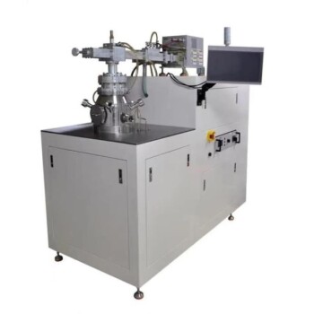
- Cylindrical Resonator MPCVD Machine System for Lab Diamond Growth
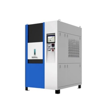
- Spark Plasma Sintering SPS Furnace
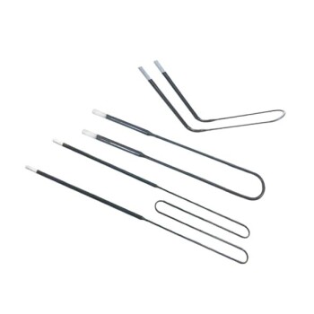
- Molybdenum Disilicide MoSi2 Thermal Heating Elements for Electric Furnace
People Also Ask
- What are the key features of MPCVD single crystal diamond deposition equipment? Precision Control for High-Quality Growth
- What is Microwave Plasma Chemical Vapor Deposition (MPCVD)? Unlock Ultra-Pure Diamond Synthesis
- What are the differences in film quality between PVD and CVD? Discover the Best Method for Your Application
- What advantages does the Laser Chemical Vapor Deposition (LCVD) process offer? High Purity & Precision SiC Fibers
- What advantages do MPCVD diamond tools offer in industrial applications? Maximize Lifespan & Efficiency


