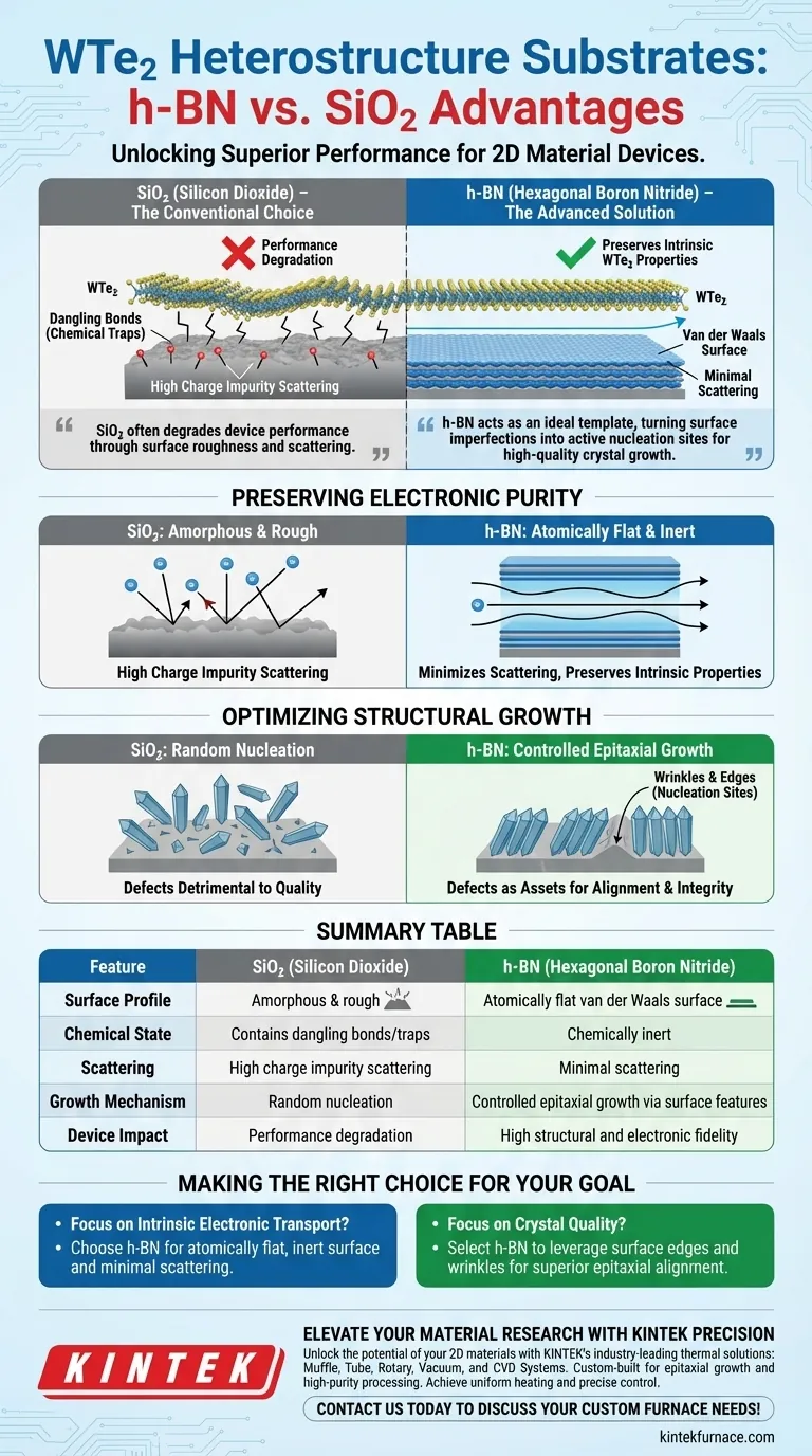
The choice of substrate fundamentally dictates the electronic fidelity of your heterostructure. High-purity hexagonal boron nitride (h-BN) outperforms silicon dioxide (SiO2) by providing an atomically flat, chemically inert surface that drastically reduces charge impurity scattering. Additionally, h-BN uniquely leverages specific surface features to promote epitaxial growth, resulting in superior structural integrity for tungsten ditelluride (WTe2) devices.
While SiO2 often degrades device performance through surface roughness and scattering, h-BN preserves the intrinsic properties of WTe2. It acts as an ideal template, turning surface imperfections into active nucleation sites for high-quality crystal growth.
Preserving Electronic Purity
The Van der Waals Interface
h-BN provides a chemically inert van der Waals surface. Unlike silicon dioxide, it provides an interface free of dangling bonds and chemical traps.
Reduction of Scattering
The atomic flatness of high-purity h-BN significantly minimizes charge impurity scattering. This allows you to preserve and observe the intrinsic electronic properties of the active WTe2 material, which are often masked by the roughness of SiO2.
Optimizing Structural Growth
Defects as Assets
On standard substrates like SiO2, surface defects are usually detrimental to device quality. However, on h-BN, specific surface defect sites—such as wrinkles or edges—serve a functional purpose.
Epitaxial Nucleation
These distinct surface features act as nucleation centers. They actively promote the epitaxial growth of tungsten ditelluride, ensuring the crystal aligns correctly during formation.
Vertical Integrity
This controlled nucleation process facilitates the creation of high-quality vertical heterostructures. The resulting material exhibits superior structural integrity compared to WTe2 grown on amorphous oxide surfaces.
Understanding the Trade-offs
Dependence on Surface Features
The advantage of h-BN relies heavily on the presence and distribution of specific surface features. The growth mechanism utilizes wrinkles and edges as seeding points.
Uniformity Considerations
If the h-BN surface is too perfect or lacks these specific nucleation centers, the epitaxial growth benefits may be diminished. You are trading the random roughness of SiO2 for a reliance on specific, localized structural cues on the h-BN surface.
Making the Right Choice for Your Goal
- If your primary focus is Intrinsic Electronic Transport: Choose h-BN to utilize its atomically flat, inert surface and minimize charge impurity scattering.
- If your primary focus is Crystal Quality: Select h-BN to leverage surface edges and wrinkles as nucleation sites for superior epitaxial alignment.
Switching to h-BN transforms the substrate from a passive mechanical support into an active component that enhances both crystal quality and electronic performance.
Summary Table:
| Feature | Silicon Dioxide (SiO2) | Hexagonal Boron Nitride (h-BN) |
|---|---|---|
| Surface Profile | Amorphous & rough | Atomically flat van der Waals surface |
| Chemical State | Contains dangling bonds/traps | Chemically inert |
| Scattering | High charge impurity scattering | Minimal scattering (preserves intrinsic properties) |
| Growth Mechanism | Random nucleation | Controlled epitaxial growth via surface features |
| Device Impact | Performance degradation | High structural and electronic fidelity |
Elevate Your Material Research with KINTEK Precision
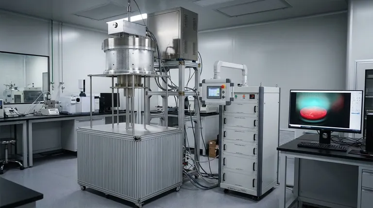
Unlock the full potential of your 2D materials and heterostructures with KINTEK’s industry-leading thermal solutions. Backed by expert R&D and manufacturing, KINTEK offers Muffle, Tube, Rotary, Vacuum, and CVD systems, all fully customizable to meet the rigorous demands of epitaxial growth and high-purity material processing. Whether you are working with h-BN substrates or developing advanced WTe2 devices, our lab high-temp furnaces provide the uniform heating and precise control necessary for superior crystal quality.
Ready to optimize your lab’s efficiency? Contact us today to discuss your custom furnace needs!
Visual Guide
References
- Andrejs Terehovs, Gunta Kunakova. Chemical Vapor Deposition for the Fabrication of WTe<sub>2</sub>/h‐BN Heterostructures. DOI: 10.1002/admi.202500091
This article is also based on technical information from Kintek Furnace Knowledge Base .
Related Products
- MPCVD Machine System Reactor Bell-jar Resonator for Lab and Diamond Growth
- Custom Made Versatile CVD Tube Furnace Chemical Vapor Deposition CVD Equipment Machine
- Vertical Laboratory Quartz Tube Furnace Tubular Furnace
- 915MHz MPCVD Diamond Machine Microwave Plasma Chemical Vapor Deposition System Reactor
- HFCVD Machine System Equipment for Drawing Die Nano Diamond Coating
People Also Ask
- How do carbon-containing groups contribute to diamond growth in the MPCVD method? Unlock High-Quality Diamond Synthesis
- What are the essential components of an MPCVD reactor system? Build a Pristine Environment for High-Purity Materials
- How can the growth rate of diamond be accelerated in the MPCVD method? Boost Growth with Higher Power & Pressure
- What role does gas flow rate play in MPCVD? Mastering Deposition Rate and Film Uniformity
- Why is temperature control important in the MPCVD growth process? Ensure High-Quality, Reliable Diamond Film Deposition


