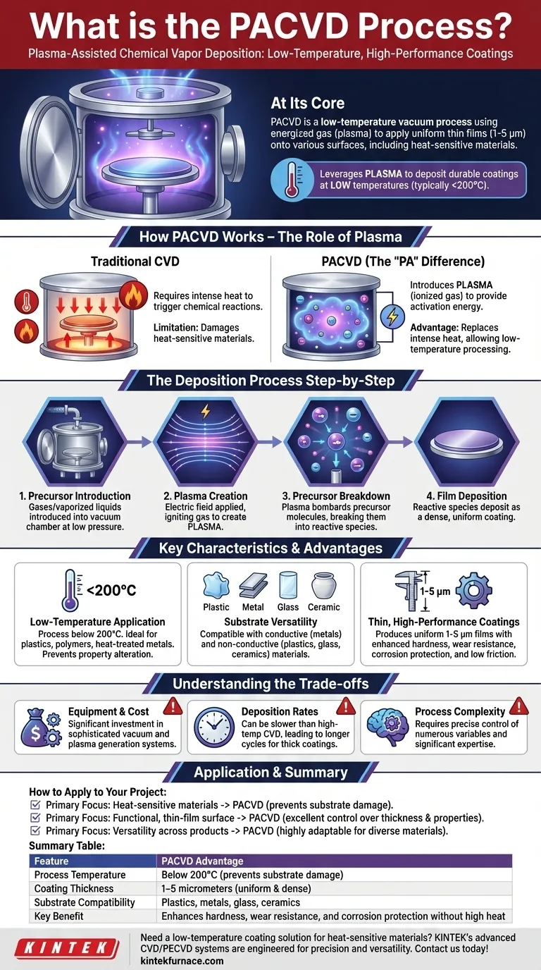
At its core, Plasma-Assisted Chemical Vapor Deposition (PACVD) is a low-temperature vacuum process used to apply thin, high-performance coatings onto a wide variety of surfaces. Unlike traditional methods that rely on intense heat, PACVD uses an energized gas (plasma) to initiate the coating reaction, allowing it to work on materials that are sensitive to high temperatures. The process typically deposits a uniform film between 1 and 5 micrometers (µm) thick.
PACVD leverages plasma to deposit durable coatings at low temperatures. This makes it possible to enhance heat-sensitive materials, such as plastics or certain alloys, that traditional high-temperature methods would damage or destroy.
How PACVD Works: The Role of Plasma
To understand PACVD, it is helpful to first understand the foundation it is built upon: Chemical Vapor Deposition (CVD).
The Foundation: Chemical Vapor Deposition
Traditional CVD processes, like Thermal CVD, involve heating a substrate in a vacuum chamber and introducing reactive gases called precursors. The high heat provides the energy needed to trigger a chemical reaction, causing a solid material to form and deposit as a thin film onto the substrate's surface.
The main limitation of this method is the requirement for very high temperatures, often many hundreds or even thousands of degrees Celsius.
The "PA" Difference: Introducing Plasma
PACVD overcomes the temperature limitation by introducing a different form of energy: plasma. Plasma is an ionized gas—a state of matter where gas atoms have been energized to the point that their electrons are stripped away.
This cloud of energized ions and electrons provides the activation energy for the chemical reaction, replacing the need for intense heat.
The Deposition Process
The PACVD process occurs in a vacuum chamber. Precursor gases or vaporized liquids are introduced into the chamber at a low pressure.
An electric field is then applied, which ignites the gas and creates plasma. This plasma bombards the precursor molecules, breaking them down into reactive species that then deposit onto the substrate as a dense, uniform coating.
Key Characteristics and Advantages
The use of plasma instead of heat gives PACVD several distinct advantages that make it suitable for a wide range of advanced applications.
Low-Temperature Application
This is the defining benefit of PACVD. With typical process temperatures below 200 °C, it is ideal for coating materials that cannot withstand high heat.
This includes plastics, polymers, and heat-treated metal components whose fundamental properties (like hardness) would be altered by a high-temperature process.
Substrate Versatility
The low-temperature nature of PACVD makes it compatible with an exceptionally broad range of materials. It is equally effective on conductive substrates like metals and non-conductive substrates like plastics, glass, and ceramics.
This flexibility allows a single process to be used for components made of vastly different materials.
Thin, High-Performance Coatings
PACVD produces very thin (typically 1–5 µm), dense, and well-adhered coatings. These films can be engineered to provide specific properties such as hardness, wear resistance, corrosion protection, or low friction.
Understanding the Trade-offs
While powerful, PACVD is not a universal solution. It's important to understand its practical limitations.
Equipment and Cost
PACVD systems require sophisticated vacuum chambers, gas handling systems, and radio-frequency (RF) or microwave power supplies to generate the plasma. This equipment represents a significant capital investment and requires specialized operational knowledge.
Deposition Rates
While highly controlled, PACVD can sometimes have lower deposition rates compared to high-temperature thermal CVD processes. For applications requiring very thick coatings, this can translate to longer cycle times.
Process Complexity
Achieving a specific coating with the desired properties requires precise control over numerous variables, including gas composition, pressure, power, and temperature. Developing a robust process for a new application requires significant expertise.
How to Apply This to Your Project
Choosing the right coating technology depends entirely on your material, budget, and performance goals.
- If your primary focus is coating heat-sensitive materials: PACVD is a leading choice because its low-temperature process prevents substrate damage to plastics, polymers, or finished metal parts.
- If your primary focus is a functional, thin-film surface: PACVD provides excellent control over film thickness and uniformity, making it ideal for creating surfaces with enhanced hardness, lubricity, or chemical resistance.
- If your primary focus is versatility across different products: The ability to coat both conductive and non-conductive materials makes PACVD highly adaptable for diverse manufacturing needs.
By understanding its unique low-temperature mechanism, you can leverage PACVD to add value and performance to materials previously considered uncoatable.
Summary Table:
| Feature | PACVD Advantage |
|---|---|
| Process Temperature | Below 200°C (prevents substrate damage) |
| Coating Thickness | 1–5 micrometers (uniform & dense) |
| Substrate Compatibility | Plastics, metals, glass, ceramics |
| Key Benefit | Enhances hardness, wear resistance, and corrosion protection without high heat |
Need a low-temperature coating solution for heat-sensitive materials? KINTEK’s advanced high-temperature furnaces and CVD/PECVD systems are engineered for precision and versatility. Leveraging our deep customization capabilities, we can tailor PACVD or other coating processes to your unique experimental requirements—whether you’re working with plastics, alloys, or ceramics. Contact our experts today to explore how our solutions can enhance your project’s performance and durability!
Visual Guide
Related Products
- RF PECVD System Radio Frequency Plasma Enhanced Chemical Vapor Deposition
- 915MHz MPCVD Diamond Machine Microwave Plasma Chemical Vapor Deposition System Reactor
- MPCVD Machine System Reactor Bell-jar Resonator for Lab and Diamond Growth
- Slide PECVD Tube Furnace with Liquid Gasifier PECVD Machine
- HFCVD Machine System Equipment for Drawing Die Nano Diamond Coating
People Also Ask
- What is the role of RF power in PECVD and how does the RF-PECVD process work? Master Thin Film Deposition Control
- How is silicon dioxide deposited from tetraethylorthosilicate (TEOS) in PECVD? Achieve Low-Temperature, High-Quality SiO2 Films
- What are the advantages of PECVD in film deposition? Achieve Low-Temp, High-Quality Coatings
- What are some promising applications of PECVD-prepared 2D materials? Unlock Advanced Sensing and Optoelectronics
- What is PECVD specification? A Guide to Choosing the Right System for Your Lab


