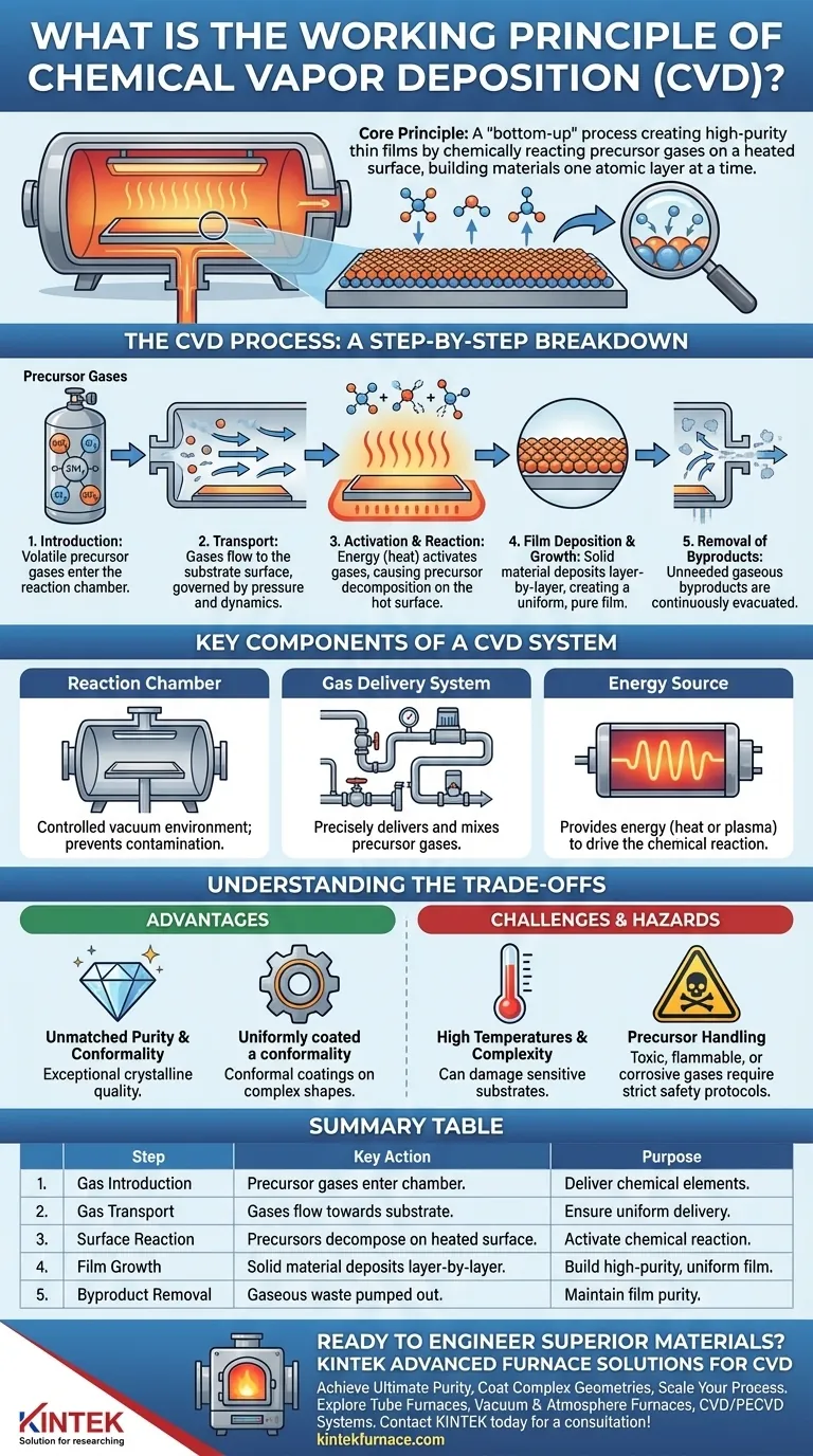
At its core, Chemical Vapor Deposition (CVD) is a "bottom-up" manufacturing process used to create high-purity, solid thin films. It works by introducing reactive gases, known as precursors, into a controlled chamber where they chemically react and deposit onto a heated surface, or substrate. This method literally builds the desired material one layer of atoms or molecules at a time.
The essential principle of CVD is not simply coating a surface, but rather orchestrating a controlled chemical reaction in a vacuum. Gaseous ingredients are transformed into a high-performance solid material directly onto a target object.
The CVD Process: A Step-by-Step Breakdown
To understand CVD, it is best to visualize it as a sequence of controlled events happening inside a specialized reactor. Each step is critical for achieving a uniform, high-quality film.
1. Introduction of Precursor Gases
The process begins by introducing precise amounts of one or more volatile precursor gases into the reaction chamber. These gases contain the chemical elements that will make up the final solid film (e.g., silane gas, SiH₄, to deposit a silicon film).
2. Transport to the Substrate
Once inside the chamber, these gases flow towards the substrate, which is the material being coated. This transport is governed by pressure and gas flow dynamics within the reactor.
3. Activation and Surface Reaction
The precursor gases must be activated, typically with energy, to make them reactive. Most often, this is done by heating the substrate to a high temperature. The hot surface provides the thermal energy needed to break down the precursor molecules when they land on it.
4. Film Deposition and Growth
As the activated precursor molecules decompose on the hot substrate, they deposit the desired solid element or compound. This creates a thin film that grows in a highly controlled, layer-by-layer fashion, ensuring excellent uniformity and purity.
5. Removal of Byproducts
The chemical reactions produce gaseous byproducts that are no longer needed. These are continuously removed from the chamber by a vacuum and exhaust system, preventing them from contaminating the growing film.
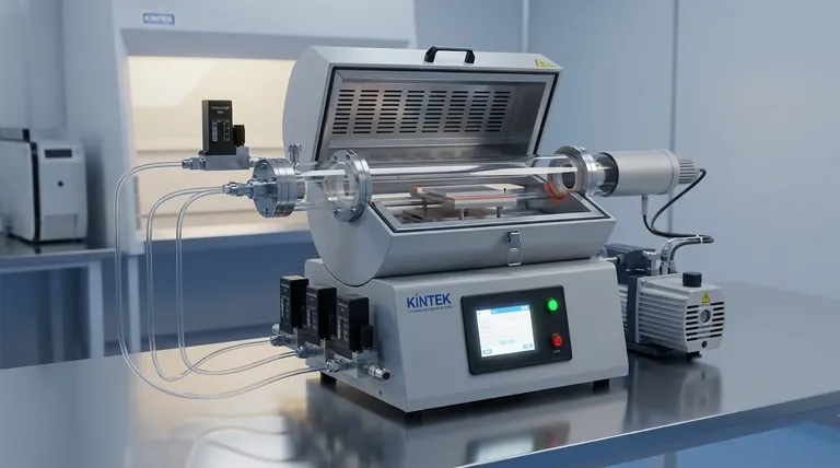
Key Components of a CVD System
A CVD system is a sophisticated piece of equipment designed to precisely manage this chemical process.
The Reaction Chamber
This is a sealed, vacuum-tight chamber that contains the entire process. The vacuum environment is critical for preventing contamination from air and for controlling the pressure, which influences gas behavior.
The Gas Delivery System
This network of pipes, valves, and mass flow controllers delivers the precursor gases into the chamber with extreme precision. The ability to control the gas mixture is fundamental to controlling the final material's properties.
The Energy Source
To drive the chemical reaction, an energy source is required. This is most commonly a heating system for the substrate, but other methods exist, such as using a plasma (as in Plasma-Enhanced CVD or PECVD), which is generated by a microwave discharge.
Understanding the Trade-offs
While powerful, CVD is not a universal solution. Understanding its advantages and limitations is key to making informed engineering decisions.
The Advantage: Unmatched Purity and Conformality
Because CVD builds a material from its fundamental chemical components, it can achieve exceptional purity and crystalline quality. It also excels at creating conformal coatings, meaning the film has a uniform thickness even over complex, non-flat surfaces.
The Challenge: High Temperatures and Complexity
Traditional thermal CVD often requires very high temperatures, which can damage sensitive substrates like certain electronics or polymers. The equipment is also complex and expensive to purchase and operate.
The Hazard: Precursor Handling
Many precursor gases used in CVD are highly toxic, flammable, or corrosive. This necessitates stringent safety protocols and specialized handling equipment, adding to the operational complexity and cost.
Making the Right Choice for Your Application
Selecting a deposition method depends entirely on your project's technical requirements and commercial constraints.
- If your primary focus is ultimate material purity and crystalline structure: CVD is often the superior choice for demanding applications like producing semiconductor wafers or synthetic diamond films.
- If your primary focus is coating complex 3D shapes uniformly: CVD's ability to deposit a conformal film makes it ideal for components like sensors, MEMS devices, and internal parts.
- If your primary focus is cost-sensitive, high-volume production on simple shapes: You must weigh the high performance of CVD against the potentially lower cost and higher throughput of alternatives like Physical Vapor Deposition (PVD) or sputtering.
Understanding the CVD principle transforms it from a black-box process into a powerful tool for precision materials engineering.
Summary Table:
| CVD Process Step | Key Action | Purpose |
|---|---|---|
| 1. Gas Introduction | Precursor gases enter the chamber. | Deliver chemical elements for the film. |
| 2. Gas Transport | Gases flow towards the substrate. | Ensure uniform delivery to the surface. |
| 3. Surface Reaction | Precursors decompose on the heated substrate. | Activate the chemical reaction for deposition. |
| 4. Film Growth | Solid material deposits layer-by-layer. | Build a high-purity, uniform thin film. |
| 5. Byproduct Removal | Gaseous waste is pumped out. | Maintain film purity and process control. |
Ready to Engineer Superior Materials with Precision Deposition?
Understanding the principle of CVD is the first step. Implementing it successfully requires a furnace system engineered for exact control, reliability, and safety.
KINTEK's advanced high-temperature furnace solutions are designed to meet the rigorous demands of CVD processes. We provide the robust, customizable thermal platforms needed to achieve the unmatched purity and conformal coatings that CVD promises.
Our expertise can help you:
- Achieve Ultimate Purity: Leverage our precise temperature control for high-quality crystalline films.
- Coat Complex Geometries: Utilize our uniform heating solutions for perfect conformal coatings on 3D parts.
- Scale Your Process: From R&D to production, our furnaces offer the reliability required for demanding applications.
Explore our product line, including Tube Furnaces, Vacuum & Atmosphere Furnaces, and specialized CVD/PECVD Systems, all backed by deep customization capabilities to fit your unique experimental requirements.
Let's discuss how we can power your next breakthrough. Contact KINTEL today for a consultation!
Visual Guide
Related Products
- Custom Made Versatile CVD Tube Furnace Chemical Vapor Deposition CVD Equipment Machine
- RF PECVD System Radio Frequency Plasma Enhanced Chemical Vapor Deposition
- MPCVD Machine System Reactor Bell-jar Resonator for Lab and Diamond Growth
- Slide PECVD Tube Furnace with Liquid Gasifier PECVD Machine
- 915MHz MPCVD Diamond Machine Microwave Plasma Chemical Vapor Deposition System Reactor
People Also Ask
- How does CVD tube furnace sintering enhance graphene growth? Achieve Superior Crystallinity and High Electron Mobility
- What improvements can be made to the bonding force of gate dielectric films using a CVD tube furnace? Enhance Adhesion for Reliable Devices
- What are the key features of CVD tube furnaces for 2D material processing? Unlock Precision Synthesis for Superior Materials
- Why are CVD tube furnace sintering systems indispensable for 2D material research and production? Unlock Atomic-Scale Precision
- What are the practical applications of gate media prepared by CVD tube furnaces? Unlock Advanced Electronics and More


