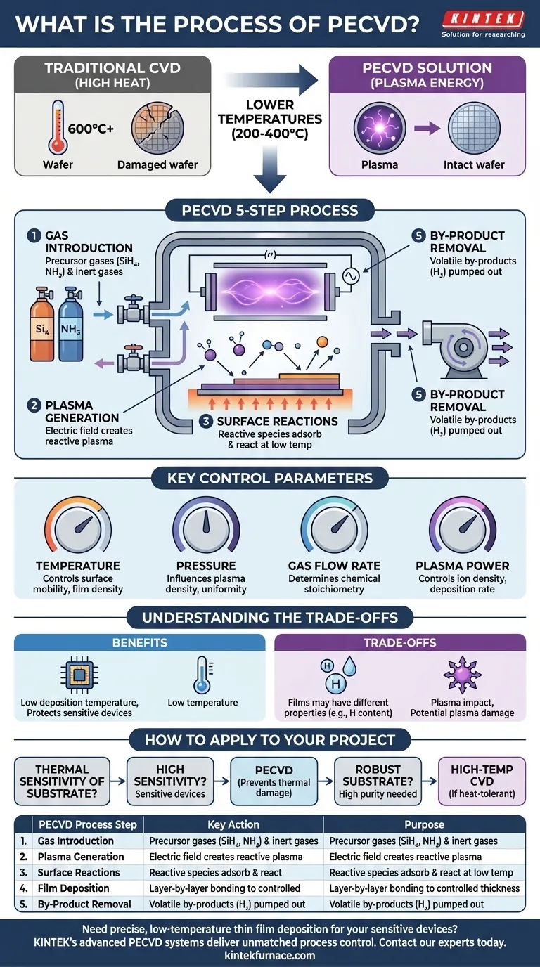
In short, the PECVD process uses an energized plasma to break down precursor gases and deposit a thin solid film onto a substrate. It is a five-step sequence: introducing reactant gases into a vacuum chamber, applying an electric field to create a plasma, allowing reactive species from the plasma to react on the substrate's surface, building the film layer by layer, and finally, removing the gaseous by-products.
The central challenge in modern device fabrication is depositing high-quality films without the damaging effects of high heat. PECVD solves this by replacing intense thermal energy with plasma energy, enabling chemical reactions to occur at significantly lower temperatures.
The Problem: Why High Temperature is a Barrier
In traditional Chemical Vapor Deposition (CVD), extreme heat (often >600°C) is the engine that drives chemical reactions. The thermal energy is necessary to break down stable gas molecules so they can react and form a film on a substrate.
However, for many advanced applications like semiconductor manufacturing, high temperatures are destructive. They can damage or alter the delicate, pre-existing patterned circuits on a silicon wafer. This thermal budget limitation created the need for a different energy source.
How PECVD Works: A Step-by-Step Breakdown
PECVD technology circumvents the heat problem by creating a low-temperature, energy-rich plasma. This is typically done within a vacuum chamber containing two parallel electrodes.
Step 1: Gas Introduction
The process begins by introducing carefully measured precursor gases into the reaction chamber. For example, to create a silicon nitride film, gases like silane (SiH₄) and ammonia (NH₃) are used, often diluted with inert gases like nitrogen.
Step 2: Plasma Generation
A high-frequency electric or magnetic field is applied across the electrodes in the chamber. This field energizes the gas mixture, stripping electrons from some of the gas molecules.
These free electrons collide with other neutral gas molecules, creating a cascade of ions and other highly reactive species. This ionized gas is the plasma, which glows and contains immense chemical potential energy without high heat.
Step 3: Surface Reactions
The reactive chemical species created in the plasma diffuse toward the heated substrate, which is typically held at a much lower temperature (200-400°C) than in traditional CVD.
These activated molecules adsorb onto the substrate surface. Because they are already in a highly reactive state, they readily undergo chemical reactions to form the desired solid material.
Step 4: Film Deposition
The products of these surface reactions bond to the substrate, forming a thin, solid film. This process continues, building the film layer by layer to a precisely controlled thickness, which can range from a few nanometers to several micrometers.
Step 5: By-product Removal
The chemical reactions also produce volatile by-products (for instance, hydrogen gas). A continuous vacuum system actively pumps these by-products out of the chamber, ensuring a clean process and pure film deposition.
Mastering the Outcome: Key Control Parameters
The quality, thickness, and properties of the deposited film are not accidental. They are controlled by precisely tuning four key process parameters.
Temperature
While PECVD is a "low-temperature" process, the substrate temperature still plays a critical role in controlling surface mobility and chemical reaction rates, which affects the final film density and stress.
Pressure
The pressure inside the chamber (typically <0.1 Torr) influences the plasma's density and the mean free path of the gas molecules. This affects the uniformity of the film across the substrate.
Gas Flow Rate
The flow rate of each precursor gas determines the chemical stoichiometry of the film. Adjusting the ratio of silane to ammonia, for example, directly changes the properties of the resulting silicon nitride film.
Plasma Power
The power applied to generate the plasma (often 100-300 eV) controls the density of ions and reactive species. Higher power can increase the deposition rate but also risks causing damage to the substrate from ion bombardment.
Understanding the Trade-offs
No technology is without compromises. The primary benefit of PECVD is its low deposition temperature, which protects sensitive devices.
The main trade-off is that films can have different properties than those grown at high temperatures. For example, PECVD silicon nitride contains a significant amount of hydrogen, which can affect its electrical properties. Furthermore, the plasma itself can sometimes cause physical damage to the substrate surface if not carefully controlled.
For many applications, these are acceptable compromises for the critical advantage of low-temperature processing.
How to Apply This to Your Project
Your choice of deposition method depends entirely on the thermal sensitivity of your substrate and your required film quality.
- If your primary focus is depositing a film on a completed device or temperature-sensitive material: PECVD is almost always the correct choice, as it prevents thermal damage.
- If your primary focus is achieving the highest possible film purity and density on a robust substrate: A high-temperature process like Low-Pressure CVD (LPCVD) might be a better option, provided your material can withstand the heat.
Ultimately, PECVD empowers the creation of complex, multi-layered devices that would be impossible to fabricate with purely thermal methods.
Summary Table:
| PECVD Process Step | Key Action | Purpose |
|---|---|---|
| 1. Gas Introduction | Introduce precursor gases (e.g., SiH₄, NH₃) | Supply reactants for film formation |
| 2. Plasma Generation | Apply electric field to create plasma | Generate reactive species without high heat |
| 3. Surface Reactions | Reactive species adsorb and react on substrate | Initiate film growth at low temperatures (200-400°C) |
| 4. Film Deposition | Layer-by-layer bonding of solid material | Build controlled thickness from nanometers to micrometers |
| 5. By-product Removal | Pump out volatile gases (e.g., H₂) | Maintain chamber purity and film quality |
Need precise, low-temperature thin film deposition for your sensitive devices? KINTEK's advanced PECVD systems leverage our deep R&D and in-house manufacturing to deliver unmatched process control. Our solutions are tailored for semiconductor, MEMS, and advanced material labs requiring high-quality films without thermal damage. Contact our experts today to discuss how our customizable PECVD technology can accelerate your project.
Visual Guide
Related Products
- Slide PECVD Tube Furnace with Liquid Gasifier PECVD Machine
- RF PECVD System Radio Frequency Plasma Enhanced Chemical Vapor Deposition
- Inclined Rotary Plasma Enhanced Chemical Deposition PECVD Tube Furnace Machine
- Inclined Rotary Plasma Enhanced Chemical Deposition PECVD Tube Furnace Machine
- Multi Heating Zones CVD Tube Furnace Machine for Chemical Vapor Deposition Equipment
People Also Ask
- In which industries is the tube furnace commonly used? Essential for Materials Science, Energy, and More
- How does PECVD equipment contribute to TOPCon bottom cells? Mastering Hydrogenation for Maximum Solar Efficiency
- How does a hydrogen reduction environment in an industrial tube furnace facilitate gold-copper alloy microspheres?
- What are the advantages of using a tube furnace CVD system for Cu(111)/graphene? Superior Scalability and Quality
- What are the main advantages of PECVD tube furnaces compared to CVD tube furnaces? Lower Temp, Faster Deposition, and More


