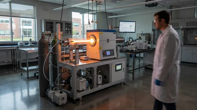
In essence, Plasma-Enhanced Chemical Vapor Deposition (PECVD) is a cornerstone technology for creating high-performance thin films on temperature-sensitive materials. Its applications span from the microchips in your smartphone to advanced optical components and the synthesis of novel materials like synthetic diamond films and carbon nanotubes. PECVD is prized for its ability to produce high-quality layers at significantly lower temperatures than traditional methods.
The core problem with traditional deposition is that creating a dense, high-quality film requires high heat, which can damage or destroy the underlying substrate. PECVD solves this by using an energy-rich plasma to drive the necessary chemical reactions, allowing for high-performance coatings at low temperatures.
The Core Principle: Why Plasma Changes the Game
To understand PECVD's applications, you must first grasp its fundamental advantage over conventional Chemical Vapor Deposition (CVD).
What is Traditional Chemical Vapor Deposition (CVD)?
Traditional CVD is like baking a cake. You introduce precursor gases (the ingredients) into a hot chamber, and the thermal energy causes them to react and deposit a solid film (the cake) onto a substrate.
This process produces excellent, high-purity films. However, it requires very high temperatures, often exceeding 600-800°C, making it unsuitable for coating materials like plastics, certain electronics, or fully fabricated semiconductor wafers.
The "Plasma-Enhanced" Advantage
PECVD adds a crucial ingredient: plasma. By applying an electric field to the gas, it creates an ionized state of matter full of highly reactive free radicals, ions, and electrons.
This plasma provides the energy needed for the chemical reactions to occur, replacing the need for intense heat. This allows deposition to happen at much lower temperatures, typically from room temperature to 350°C.
Key Application Domains
This low-temperature capability opens up a vast range of applications that are impossible with high-heat methods.
Semiconductors and Electronics
PECVD is indispensable in modern electronics. It is used to deposit dielectric films, such as silicon dioxide (SiO₂) and silicon nitride (SiNₓ), which act as insulators and protective layers between the metal interconnects of a chip.
This is critical in semiconductor manufacturing, where underlying transistors would be damaged by the high heat of traditional CVD. It is also used in consumer electronics, automotive sensors, and smart devices.
Advanced Optics
The ability to create precise, multi-layer coatings is vital for optics. PECVD is used to deposit anti-reflective coatings on lenses and solar cells, improving light transmission and efficiency.
It is also used for creating specialized coatings for optical fibers used in communications and hydrophobic (water-repellent) layers for displays and sensors.
Advanced Material Synthesis
PECVD is a powerful tool for research and development. Specialized microwave PECVD systems are used to grow high-purity materials that require specific crystalline structures.
This includes the synthesis of polycrystalline diamond films for industrial cutting tools or thermal management, as well as the growth of carbon nanotubes and nanowires for next-generation electronics and composites.
Protective and Functional Coatings
The low-temperature process allows for coating a wide variety of materials, including polymers and metals. This is used to create biocompatible coatings for medical implants and biosensors.
It also enables the deposition of hard, scratch-resistant, or corrosion-resistant films on items that cannot withstand high temperatures.
Understanding the Trade-offs
While powerful, PECVD is not a universal solution. An objective assessment requires understanding its limitations.
Film Quality and Purity
Because plasma is used to break down precursor gases like silane (SiH₄), PECVD films often contain a significant amount of incorporated hydrogen. This can affect the film's electrical properties and long-term stability.
Achieving the purity of a high-temperature thermal process can be challenging, as the plasma environment can be complex to control perfectly.
Process Complexity and Stress
PECVD systems are more complex than traditional CVD reactors, requiring vacuum chambers, gas handling, and RF or microwave power sources to generate the plasma.
While films are often described as "low-stress," improper process parameters can still result in high internal stress, leading to poor adhesion or film cracking. Careful tuning is required.
Making the Right Choice for Your Project
Your choice of deposition technology should be driven by your substrate and your desired film properties.
- If your primary focus is ultimate purity for a resilient substrate: Consider traditional high-temperature CVD or Atomic Layer Deposition (ALD).
- If your primary focus is depositing a dielectric or passivation layer on a finished electronic device: PECVD is the industry-standard choice due to its low-temperature process.
- If your primary focus is creating multi-layer optical coatings on glass or plastic: PECVD offers the control and low temperatures necessary for this task.
- If your primary focus is growing novel materials like diamond or nanotubes at low temperatures: A specialized PECVD system is the enabling technology.
Ultimately, understanding that PECVD's value lies in decoupling the deposition energy from thermal heat empowers you to leverage it for projects that would otherwise be impossible.
Summary Table:
| Application Domain | Key Materials Deposited | Primary Benefit |
|---|---|---|
| Semiconductors & Electronics | Silicon Dioxide (SiO₂), Silicon Nitride (SiNₓ) | Low-temperature insulation & passivation for sensitive devices |
| Advanced Optics | Anti-reflective coatings, hydrophobic layers | Enhanced light transmission & surface functionality |
| Advanced Material Synthesis | Polycrystalline diamond, carbon nanotubes | Low-temperature growth of high-purity crystalline materials |
| Protective & Functional Coatings | Biocompatible, scratch/corrosion-resistant films | Coating of temperature-sensitive substrates (polymers, metals) |
Need a high-performance PECVD solution tailored to your unique requirements?
At KINTEK, we leverage our exceptional R&D and in-house manufacturing capabilities to provide advanced PECVD systems for diverse laboratories. Whether you are developing next-generation semiconductors, precision optical coatings, or synthesizing novel materials like diamond films, our deep customization expertise ensures your furnace solution precisely meets your experimental needs.
Contact our experts today to discuss how our PECVD technology can accelerate your project!
Visual Guide

Related Products
- RF PECVD System Radio Frequency Plasma Enhanced Chemical Vapor Deposition
- Slide PECVD Tube Furnace with Liquid Gasifier PECVD Machine
- MPCVD Machine System Reactor Bell-jar Resonator for Lab and Diamond Growth
- 915MHz MPCVD Diamond Machine Microwave Plasma Chemical Vapor Deposition System Reactor
- Inclined Rotary Plasma Enhanced Chemical Deposition PECVD Tube Furnace Machine
People Also Ask
- How are deposition rates and film properties controlled in PECVD? Master Key Parameters for Optimal Thin Films
- What is RF in PECVD? A Critical Control for Plasma Deposition
- How is silicon dioxide deposited from tetraethylorthosilicate (TEOS) in PECVD? Achieve Low-Temperature, High-Quality SiO2 Films
- What are some promising applications of PECVD-prepared 2D materials? Unlock Advanced Sensing and Optoelectronics
- What are the key advantages of PECVD technology? Achieve Low-Temperature, High-Quality Thin Film Deposition


